Light emitting diode and method of fabricating thereof
a technology of light-emitting diodes and diodes, which is applied in the direction of basic electric elements, electrical equipment, semiconductor devices, etc., can solve the problem that the formed photons are not easily released, and achieve the effect of increasing the efficiency of light extraction
- Summary
- Abstract
- Description
- Claims
- Application Information
AI Technical Summary
Benefits of technology
Problems solved by technology
Method used
Image

Examples
first embodiment
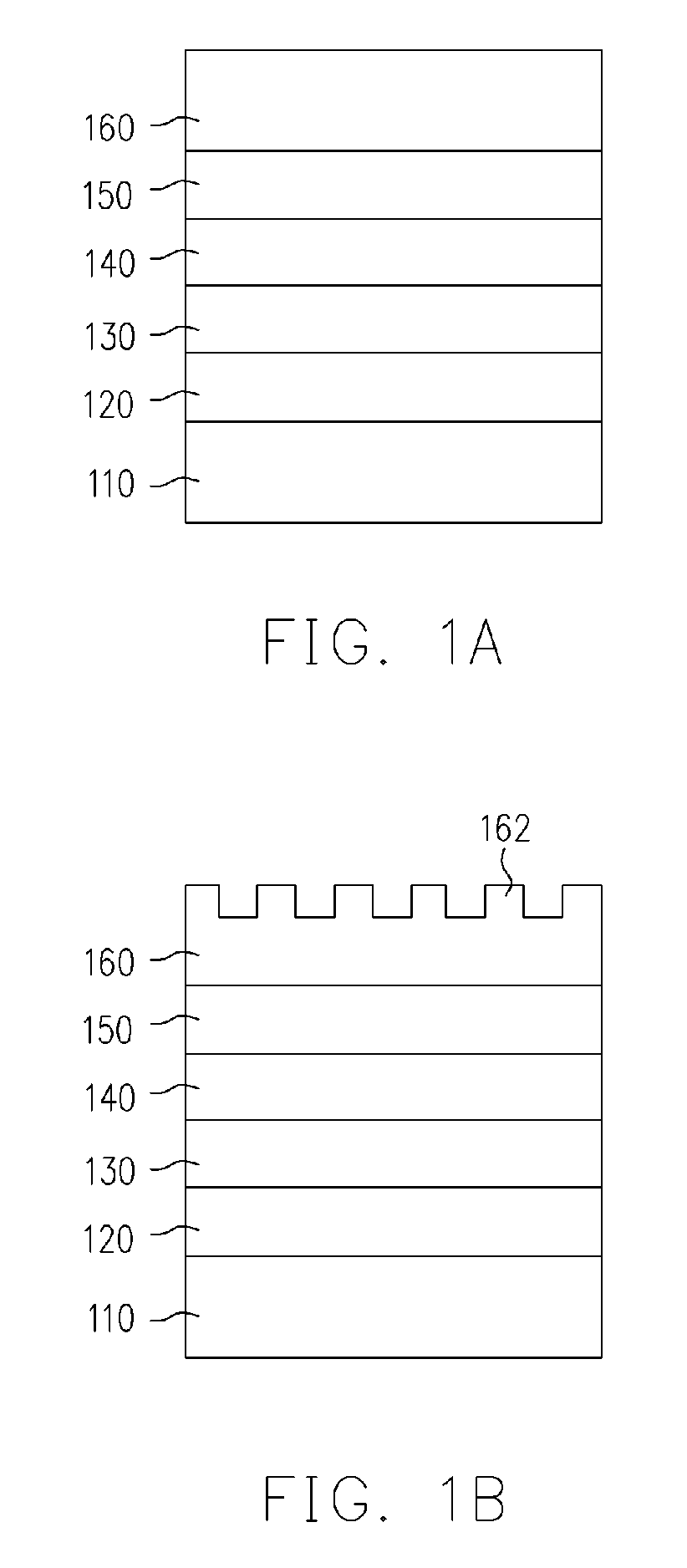
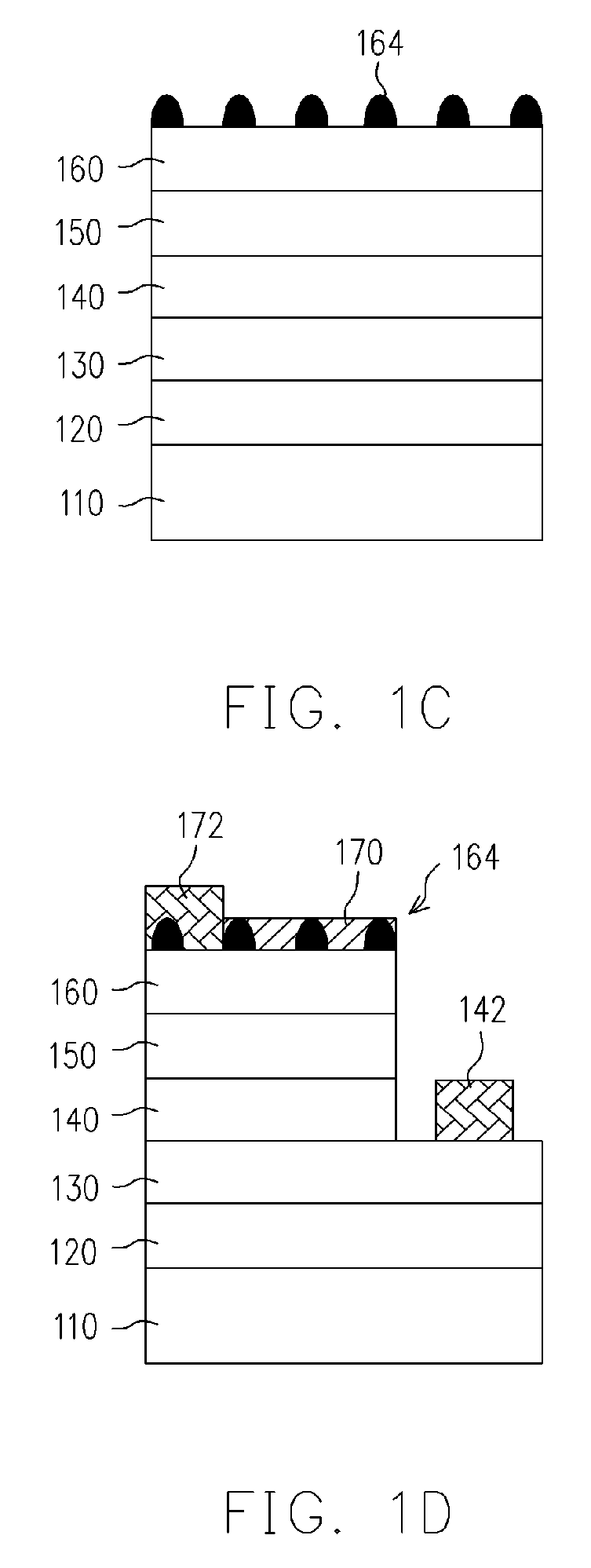
[0033]FIG. 1A to FIG. 1D are cross-sectional diagrams schematically illustrating the fabrication process of the light emitting diode, according to the present invention, wherein the FIG. 1D is a finished structure diagram for the light emitting diode.
[0034] Referring to FIG. 1A, an epitaxial structure 120-160 is first provided on a substrate 110. In this embodiment, the material of the substrate 110 is a C-Plane sapphire, R-Plane sapphire, A-Plane sapphire, SiC (for example, 6H—SiC or 4H—SiC), other materials that are suitable to be used as the substrate 110 including Si, ZnO, GaAs or MgAl2O4, or single crystalline compounds with lattice constant substantially the same as the semiconductor nitride. And the method for forming the epitaxial structure is the sequential forming of a buffer layer 120, a first contact layer 130, an active layer 140, a clad layer 150, and a second contact layer 160 on a substrate 110, wherein the buffer layer 120 may be fabricated, for example, from any of...
second embodiment
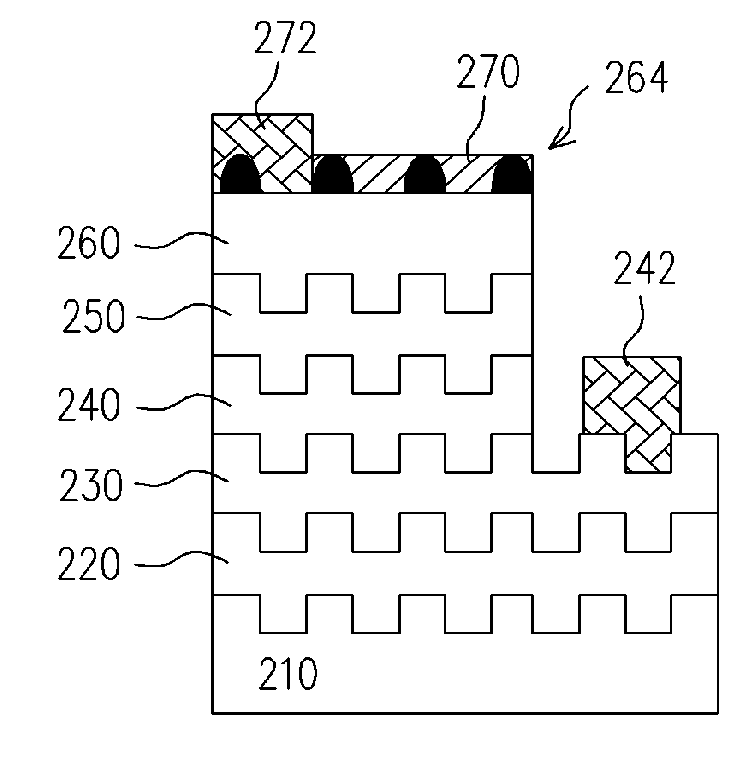
[0040]FIG. 2A to FIG. 2C are cross-sectional diagrams schematically illustrating the fabrication process of the light emitting diode, according to the present invention, wherein FIG. 2C is a finished structure diagram for the light emitting diode.
[0041] Referring to FIG. 2A, a surface patterned substrate 210 is first provided for use as the substrate in this embodiment, wherein a surface pattern 212, a buffer layer 220, a first contact layer 230, an active layer 240, a clad layer 250, and a second contact layer 260 are sequentially formed above the surface for the surface patterned substrate 210. Because each of the aforementioned layers (including the buffer layer 220, the first contact layer 230, the active layer 240, the clad layer 250, and the second contact layer 260) is influenced by the surface pattern 212 of the surface patterned substrate 210, a plurality of first patterns 262 are therefore formed on the second contact layer 260. And the materials for the aforementioned sub...
third embodiment
[0045]FIG. 3A to FIG. 3C are cross-sectional diagrams schematically illustrating the fabrication process of the light emitting diode, according to the present invention, wherein FIG. 3C is a finished structure diagram for the light emitting diode.
[0046] Referring to FIG. 3A, a buffer layer 320, a first contact layer 330, an active layer 340, and a clad layer 350 are formed above a substrate 310 in this embodiment. Thereafter, a second contact layer 360 is formed on the clad layer 350, and using the changes of the epitaxial conditions, a plurality of first patterns 362 are allowed to be formed on the second contact layer 360.
[0047] Later, referring to FIG. 3B, using the mass transfer method, the first pattern 362 undergoes deformation and a plurality of second patterns 364 are formed, wherein a surface topography of the second pattern 364 is smoother and more gradual than that of the first pattern 362. And the second pattern 364 is a mass transferred pattern. In this embodiment, the...
PUM
 Abstract
Description
Claims
Application Information
 - R&D
- Intellectual Property
- Life Sciences
- Materials
- Tech Scout
- Unparalleled Data Quality
- Higher Quality Content
- 60% Fewer Hallucinations
Browse by: Latest US Patents, China's latest patents, Technical Efficacy Thesaurus, Application Domain, Technology Topic, Popular Technical Reports.
© 2025 PatSnap. All rights reserved.Legal|Privacy policy|Modern Slavery Act Transparency Statement|Sitemap|About US| Contact US: help@patsnap.com