System and method for sensing capacitance change of a capacitive sensor

a capacitive sensor and capacitive feedback technology, applied in the field of capacitive sensing circuits, can solve the problems of large parasitic capacitance at the connection, significant influence, and charge trapped inside, and achieve the effects of reducing power consumption, high signal-to-noise ratio, and small footprin

Inactive Publication Date: 2006-12-07
GEORGIA TECH RES CORP
View PDF6 Cites 60 Cited by
  • Summary
  • Abstract
  • Description
  • Claims
  • Application Information

AI Technical Summary

Benefits of technology

[0019] Exemplary embodiments of the present invention overcome the deficiencies in the prior art by providing systems and methods for sensing the capacitance change of a capacitive sensor and for optimizing a capacitive sensing circuit. A capacitance sensing circuit, in accordance with the present invention, can sense minute capacitance change with the presence of a large parasitic capacitance. The circuit may be adapted to reduce power consumption, create a smaller footprint, provide a high signal to noise ratio (SNR), and improve linearity.
[0020] In a first exemplary embodiment, the capacitive sensing circuit may include a capacitive sensor, a programming circuit, and an amplifier. The capacitive sensor produces an output that is coupled to the amplifier. The connecting node between the capacitive sensor and the amplifier is a floating node. The floating node may also be connected to the programming circuit for controlling the charge on the floating node. Such control of the charge on the floating node helps the circuit achieve greater precision in a smaller package. In some embodiments, the floating node may also be coupled to ground through a parasitic capacitor. The programming circuit may be adapted to control a charge on the floating node.
[0022] In accordance with another embodiment of the present invention relates a method of controlling a charge on a floating node, whereby using a programming transistor is provided. The programming transistor may include a source, a floating gate, and a drain. The method includes applying a first predetermined voltage signal to the source of the programming transistor, applying a second predetermined voltage signal to the floating gate of the programming transistor, and applying a third predetermined voltage signal to the drain of the programming transistor until a charge on the floating gate of the programming transistor reaches a predetermined value. The charge on the floating gate of the programming transistor may drive the charge on the floating node to the predetermined value. Accordingly, the charge on the floating node can be controlled.

Problems solved by technology

When connecting a sensor to an amplifier, there is usually a large parasitic capacitance at the connection.
Thus, it may be significantly affected by the parasitic capacitance.
Charges may be trapped inside or may hop through a leaky medium of the sensor.
Further, the charges may leak out from bonding sites and form undesired leakage currents.
Therefore, the charge on the connecting node is unpredictable.
Sensing the minute capacitor variation, dealing with the large parasitic capacitance and leakage currents, and providing the output signal with large dynamic range makes the interface circuit design a challenge.
It is even more difficult if low power consumption is desired.
This approach consumes lots of power, usually in the range of milli-Watts (mW), and the circuits are typically be complicated and consume a large area.
In this approach, the charge-sharing and clock feed-through perturbations resulting from the switches degrade the circuit performance.
Additionally, the high frequency clocks also make this design more complicated than desired, and consume more power.
Moreover, the use of switches causes the design to take up more space than desired.
Additionally, both designs are prone to the effect of the parasitic capacitance from the connecting node to the ground.

Method used


Image

  • System and method for sensing capacitance change of a capacitive sensor
  • System and method for sensing capacitance change of a capacitive sensor
  • System and method for sensing capacitance change of a capacitive sensor

Examples


Embodiment Construction

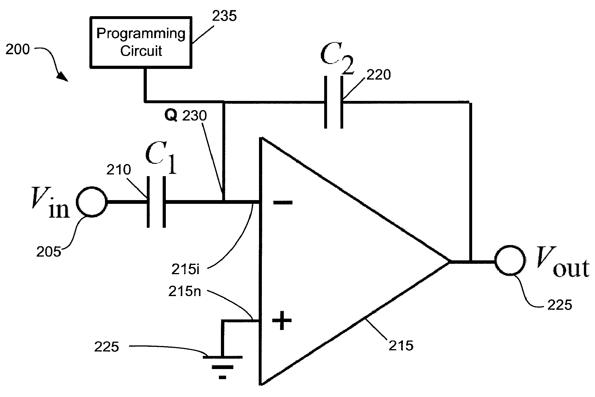
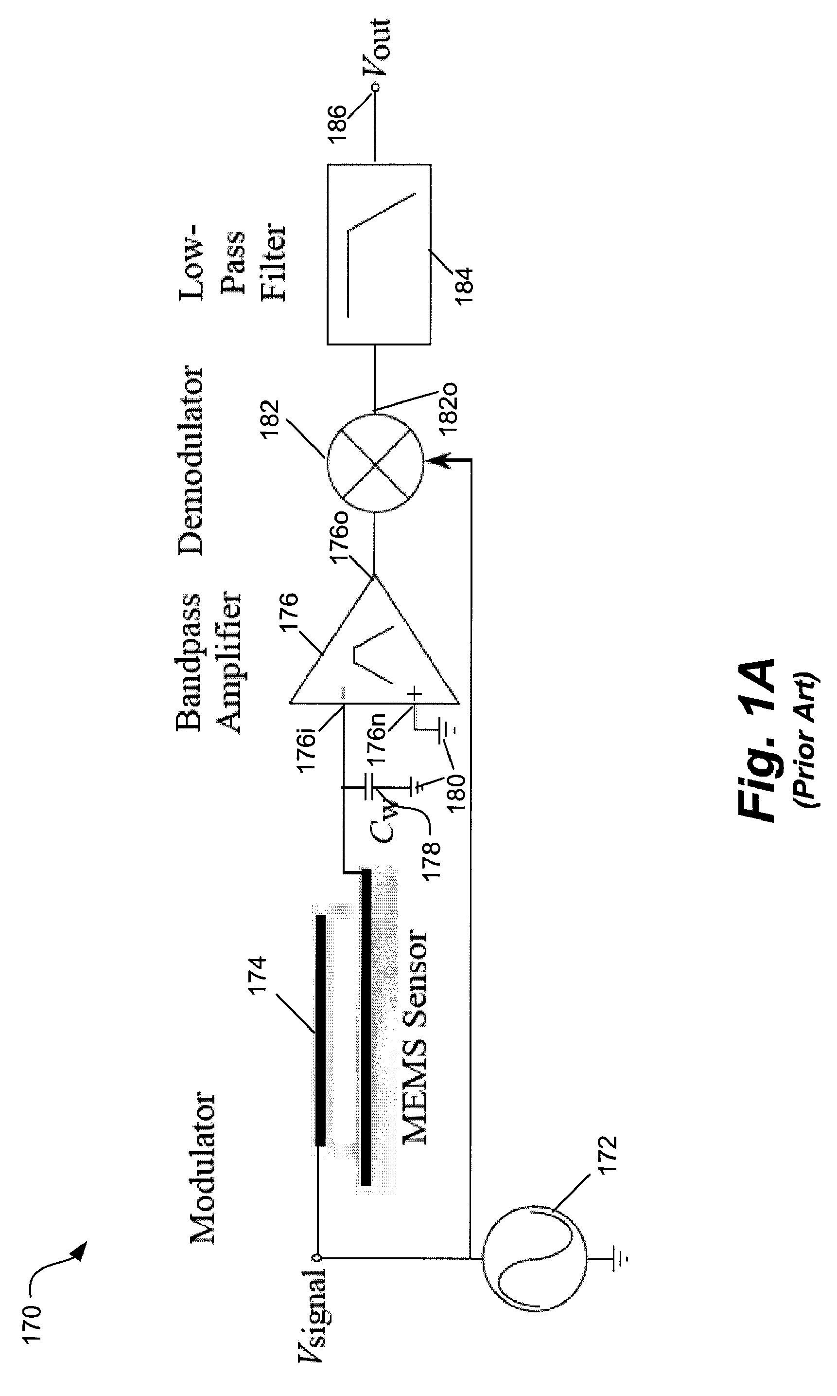
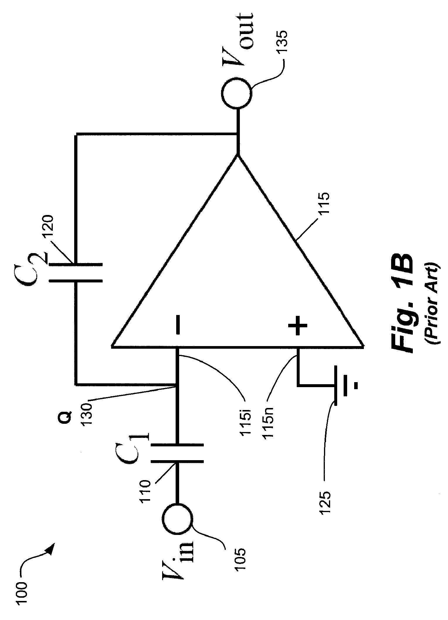
[0047] To facilitate an understanding of the principles and features of the invention, it is explained hereinafter with reference to its implementation in illustrative embodiments. In particular, the present invention is directed towards systems and methods for sensing the capacitance change of a capacitive sensor.

[0048] Referring now to the figures, wherein like reference numerals represent like parts throughout the several views, exemplary embodiments of the present invention will be described in detail. Throughout this description, various components may be identified having specific values, these values are provided as exemplary embodiments and should not be limiting of various concepts of the present invention as many comparable sizes and / or values may be implemented.

[0049] Floating gate transistors can be a valuable tool in circuit design because floating gates can be used to create many discrete analog circuits using only capacitor based components. This is very useful, bec...


PUM


Abstract

The present invention relates to systems and methods for sensing capacitance change of a capacitive sensor and for optimizing a capacitive sensing circuit. In an exemplary embodiment, a capacitive sensor may be coupled to an amplifier at floating node. A programming circuit is connected to the floating node for controlling a charge on the floating node. A method of controlling the charge of the floating node is also provided. The method includes applying a first predetermined voltage to a source of a programming transistor, applying a second predetermined voltage to a floating gate of the programming transistor, and applying a third predetermined voltage to a drain of the programming transistor until a charge on the floating gate of the programming transistor reaches a predetermined value. The charge on the floating gate of the programming transistor drives the charge on the floating node to the predetermined value, and thus is controlled.

Description

CROSS REFERENCE TO RELATED APPLICATION [0001] This application claims priority of U.S. Provisional Patent Application No. 60 / 686,825, filed 2 Jun. 2005, the entire contents of which is hereby incorporated by reference.BACKGROUND [0002] 1. Field of the Invention [0003] The present invention is related to a capacitive sensing circuit and, more particularly, to a capacitive feedback amplifier with a floating-node charge programming circuit for sensing capacitance change of a capacitive sensor. [0004] 2. Description of Related Art [0005] In the design of Microsystems, it is frequently desirable to utilize sensors to transduce some information into electrical signals which can be processed by the circuit. Such sensors sense various types of signals and may be used for capturing information such as temperature, pressure, voltage, capacitance, resistance, or the like. For example, the sensor may be a MEMS sensor, a CMUT (capacitive micro-machined ultrasonic transducer), a temperature senso...

Claims


Application Information

Patent Timeline
Patent Type & Authority Applications(United States)
IPC IPC(8): G01R27/26
CPCG01D5/24G01R27/2605G01K7/34
Inventor PENG, SHENG-YUHASLER, PAUL E.
Owner GEORGIA TECH RES CORP
Why Eureka
Try Eureka