

Method for manufacturing a semiconductor device having a STI structure
- Summary
- Abstract
- Description
- Claims
- Application Information
AI Technical Summary
Benefits of technology
Problems solved by technology
Method used
Image

Examples
first embodiment
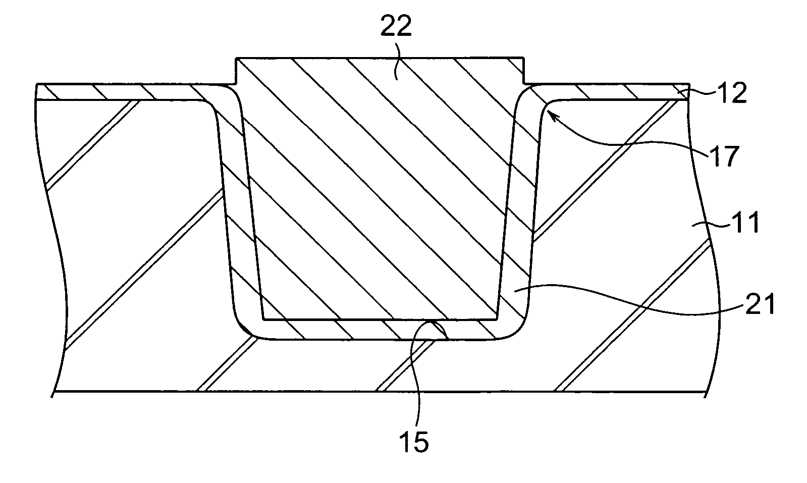
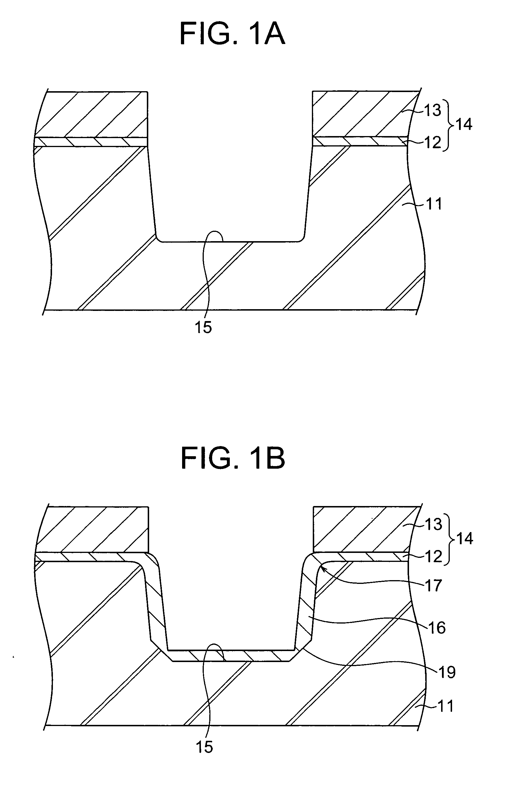
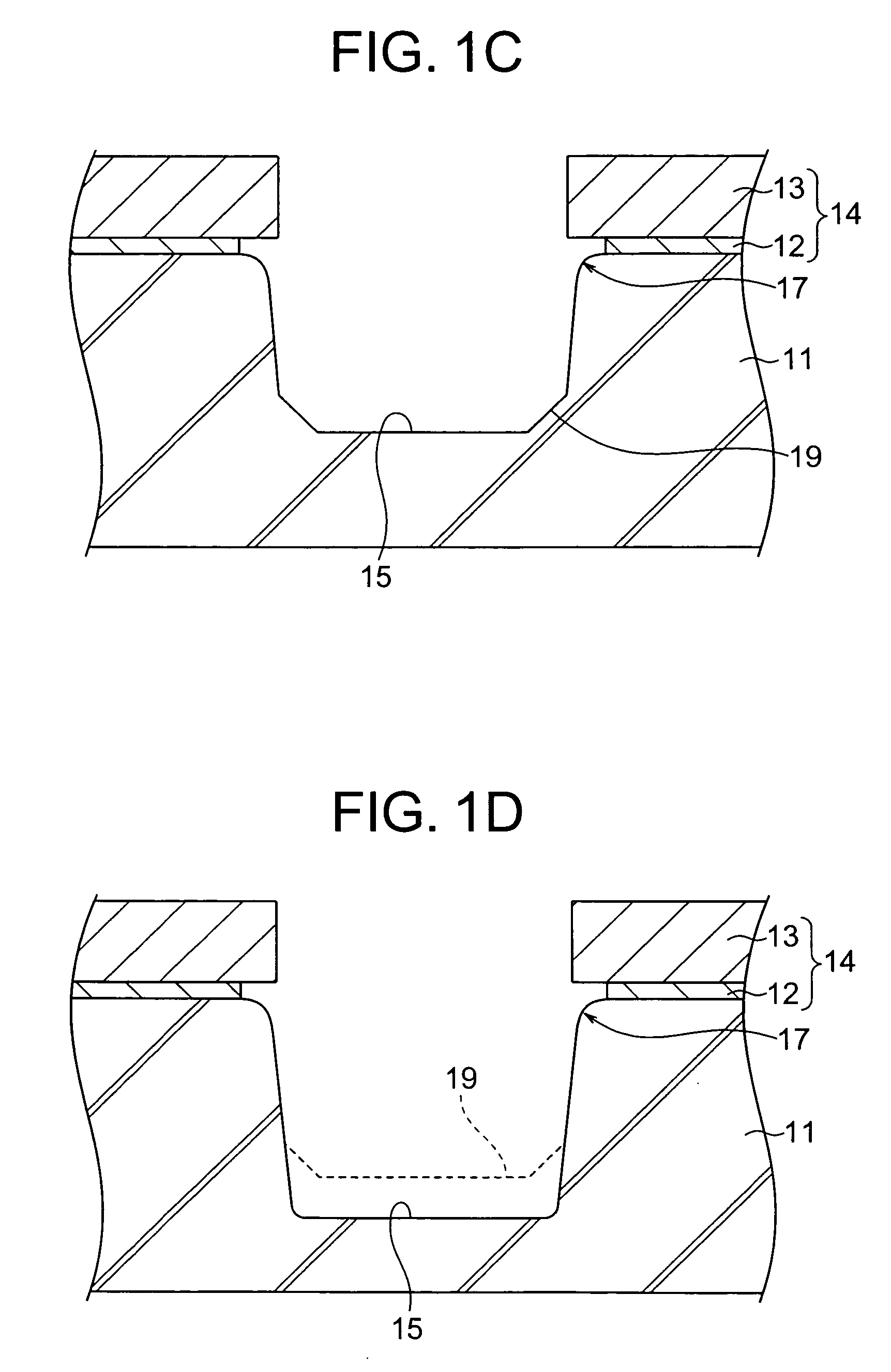
[0031]FIGS. 1A to 1H are sectional views showing consecutive steps of manufacturing a semiconductor device according to the present invention. First, an about 10-nm-thick pad oxide film 12 made of silicon oxide and an about 150-nm-thick pad nitride film 13 made of silicon nitride are consecutively formed on a silicon substrate 11. Subsequently, by using a known technique, the pad nitride film 13 and pad oxide film 12 are etched to form a combination mask 14 having a desired opening pattern. Then, a first anisotropic etching process is conducted using the mask 14 as an etching mask, to form a trench 15 having a depth of 200 nm as measured from the top surface of the silicon substrate 11, thereby obtaining the structure shown in FIG. 1A.
[0032] The first anisotropic etching process is conducted in an etching gas including O2, HBr and Cl2 and at a gas pressure of 10 to 50 Torr. The taper angle of the sidewall of the trench 15 with respect to a perpendicular to the main surface of the si...
second embodiment
[0049]FIGS. 6A to 6E show consecutive steps of manufacturing a semiconductor device according to the present invention. In this embodiment, the present invention is applied to a process for forming a gate electrode in a recessed channel array transistor. In the recessed channel array transistor, the gate electrode of a MOSFET has a portion received in a trench formed on the surface region of the silicon substrate, whereby the channel of the MOSFET extends along the bottom surface region of the trench to have a larger channel length.
[0050] A device isolation structure 23 is first formed on the surface region of a silicon substrate 11, followed by a thermal oxidation process to form an about 10-nm-thick protective oxide film 41 on the device region of the silicon substrate 11. Thereafter, a nitride film 42 is deposited to a thickness of 100 nm on the protective oxide film 41 by a CVD process. The protective oxide film 41 is formed to intervene in the direct contact between the silicon...
PUM
 Abstract
Description
Claims
Application Information