

Macroporous silicon microcavity with tunable pore size
a micro-cavity and micro-pore technology, applied in the field of macro-cavity structures, can solve the problems of lack of sensitivity, time-consuming and inconvenient procedures, limited quantitative analysis of such analytes, etc., and achieve the effect of greater sensitivity in sensing
- Summary
- Abstract
- Description
- Claims
- Application Information
AI Technical Summary
Benefits of technology
Problems solved by technology
Method used
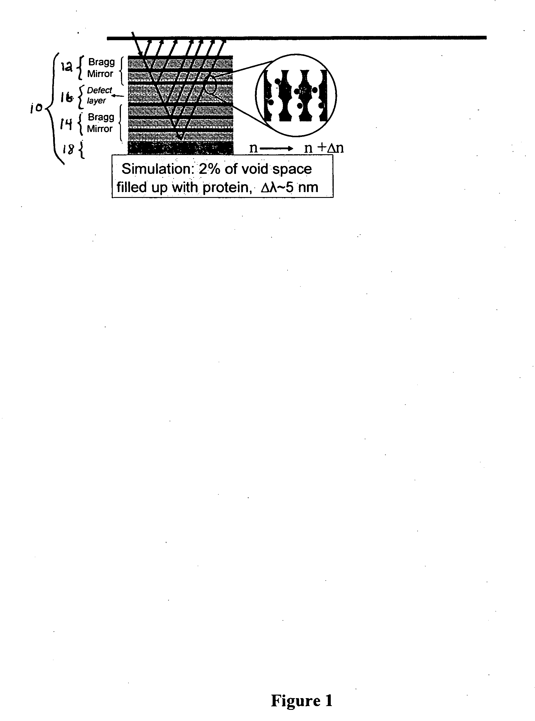
Image

Examples
example 1
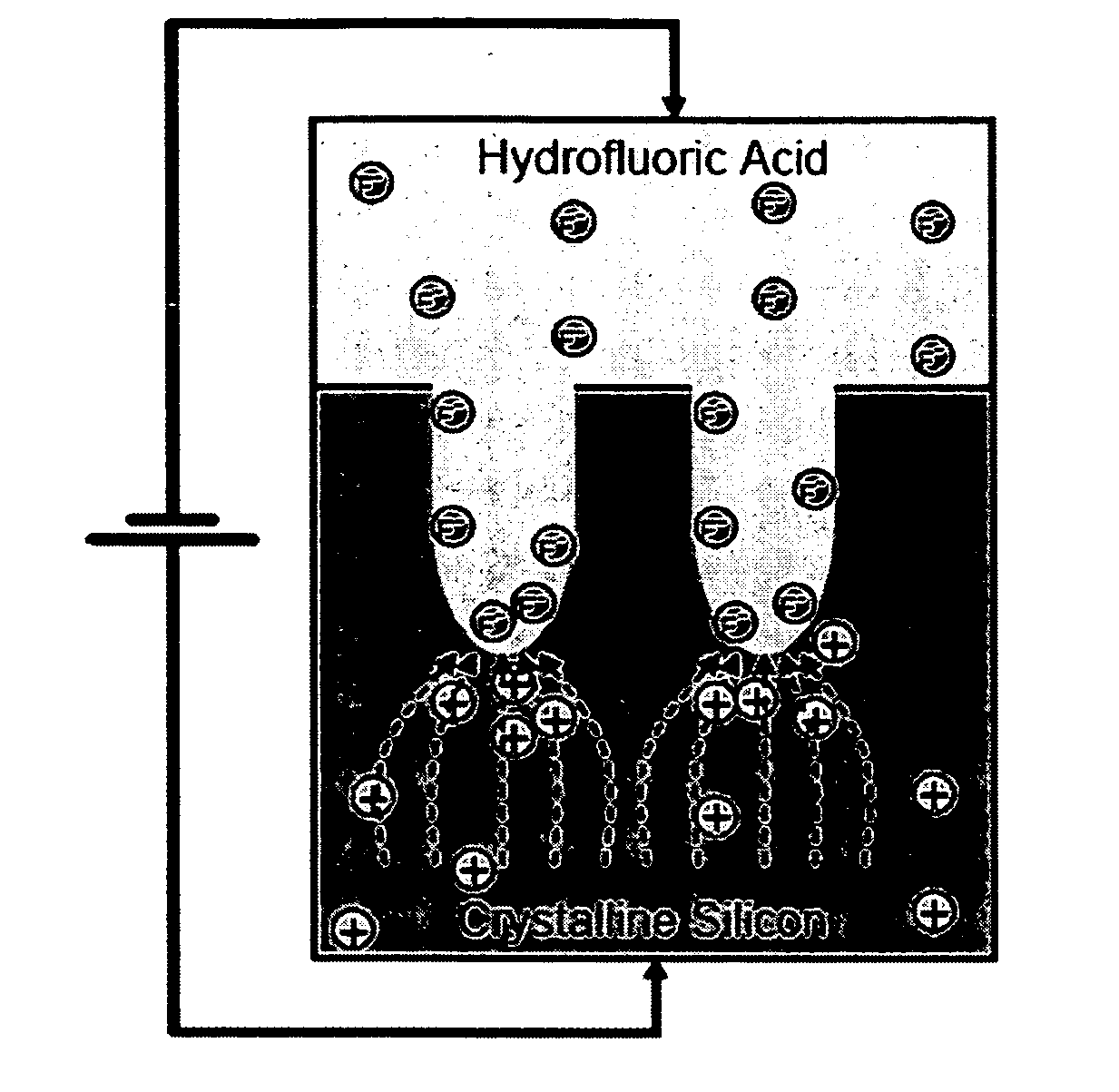
Fabrication of Macroporous Silicon Microcavity (Pores<300 nm) in n-Type Silicon
[0102] The general trend in n-type PSi is that the pore density increases as the substrate doping level increases (Theunissen, “Etch Channel Formation During Anodic Dissolution of n-Type Silicon in Aqueous Hydrofluoric Acid ,”J. Electrochem. Soc. 119:351-360 (1972); Lehmann et al., “On the Morphology and the Electrochemical Formation Mechanism of Mesoporous Silicon,”Mater. Sci. Eng. B 69(70):11-22 (2000); Lehmann & Föll, “Formation Mechanism and Properties of Electrochemically Etched Trenches in n-Type Silicon,”J. Electrochem. Soc. 137:653-659 (1990), which are hereby incorporated by reference in their entirety). However, only well-defined macropores with pore sizes larger than 300 nm (Schilling et al., “Optical Characterisation of 2D Macroporous Silicon Photonic Crystals With Bandgaps Around 3.5 and 1.3 μm,”Opt. Mater. 17(1-2):7-10 (2001); Lehmann & Gruning, “The Limits of Macropore Array Fabrication,”T...
example 2
Fabrication of Mesoporous Silicon Microcavity on p-Type Silicon
[0105] As shown in FIGS. 5A-B, a mesoporous silicon microcavity with an average pore diameter of approximately 20 nm was formed in a highly doped p-type silicon substrate (0.01 ohm-cm) using an electrolyte with 15% HF in ethanol. The mesopores formed in p+silicon substrates have highly branched pore walls. The 20 nm pore size is suitable for detection of small objects such as short DNA segments and low molecular weight molecules.
example 3
Fabrication of Large Macroporous Silicon Structures
[0106] A large single-layer macroporous (1.5 μm) structure was etched from low doped p-type silicon (20 ohm-cm) using an HF / dimethylformamide electrolyte (Haurylau et al., “Optical Properties and Tunability of Macroporous Silicon 2-D Photonic Bandgap Structures,”Phys. Stat. Sol. A 202(8):1477-1481 (2005), which is hereby incorporated by reference in its entirety). As shown in FIGS. 6A-B, it has substantially straight and smooth pores.
[0107] Very large macropores (pore size of ˜2 μm) etched from low doped p-type silicon (20 ohm-cm) using an HF / dimethylformamide electrolyte are shown in FIG. 7 (Haurylau et al., “Optical Properties and Tunability of Macroporous Silicon 2-D Photonic Bandgap Structures,”Phys. Stat. Sol. A 202(8): 1477-1481 (2005), which is hereby incorporated by reference in its entirety). The large macropores are tunable from 500 nm to 10 microns, which is suitable for the detection of very large objects such as bacte...
PUM
 Abstract
Description
Claims
Application Information