Perovskite-based thin film structures on miscut semiconductor substrates

a technology of semiconductor substrates and thin films, applied in the field of semiconductors, can solve the problems of significantly reducing piezoelectric qualities of piezoelectric crystalline materials grown on semiconductor substrates such as silicon, and achieve the effects of high saturation strain, high quality epitaxial heterostructures, and good metallic behavior

Inactive Publication Date: 2006-12-28
PENN STATE RES FOUND +1
View PDF13 Cites 235 Cited by
  • Summary
  • Abstract
  • Description
  • Claims
  • Application Information

AI Technical Summary

Benefits of technology

[0011] Some ofthe present structures include a first perovskite overlayer disposed over the perovskite seed layer, a second perovskite overlayer disposed over the first perovskite overlayer and, optionally, a third perovskite overlayer disposed over. the second perovskite overlayer. In one such embodiment, the second perovskite overlayer is composed of a piezoelectric material and the first and third perovskite overlayers provide electrodes sandwiching the piezoelectric perovskite overlayer. However, electrodes other than perovskite-based electrodes may also be used. Examples of perovskites that may be used to make the electrodes include SrRuO3 and CaRuO3. SrRuO3 is a preferred electrode material for use with PMN-PT-based structures due to its small lattice mismatch with PMN-PT (33%), which allows the growth of high quality epitaxial heterostructures with SrRuO3 electrodes. In addition, SrRuO3 is stable up to 1200K i

Problems solved by technology

However, piezoelectric crystalline materials grown on semiconductor substrates such as silicon often have

Method used


Image

  • Perovskite-based thin film structures on miscut semiconductor substrates
  • Perovskite-based thin film structures on miscut semiconductor substrates
  • Perovskite-based thin film structures on miscut semiconductor substrates

Examples


example 1

Fabrication of a PMN-PT-Based Piezoelectric Thin Film Structure

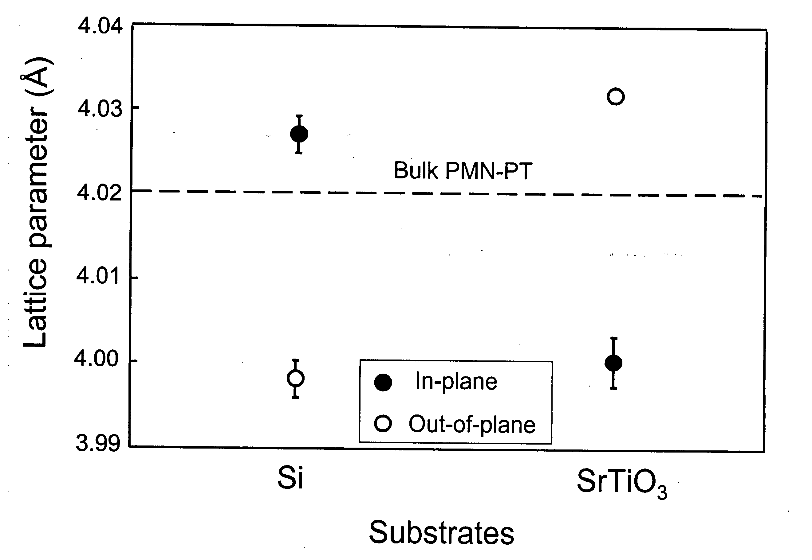
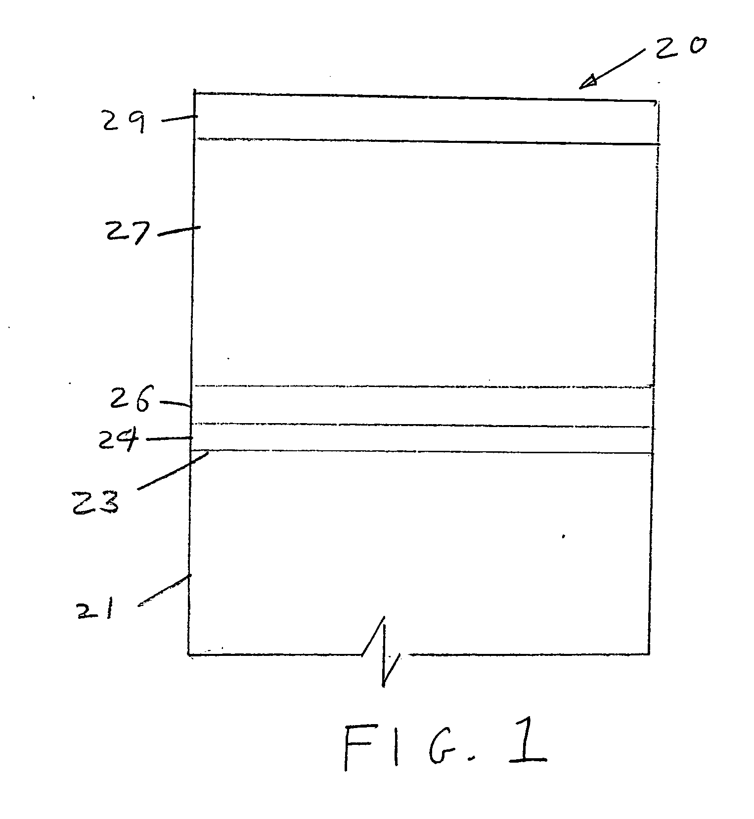
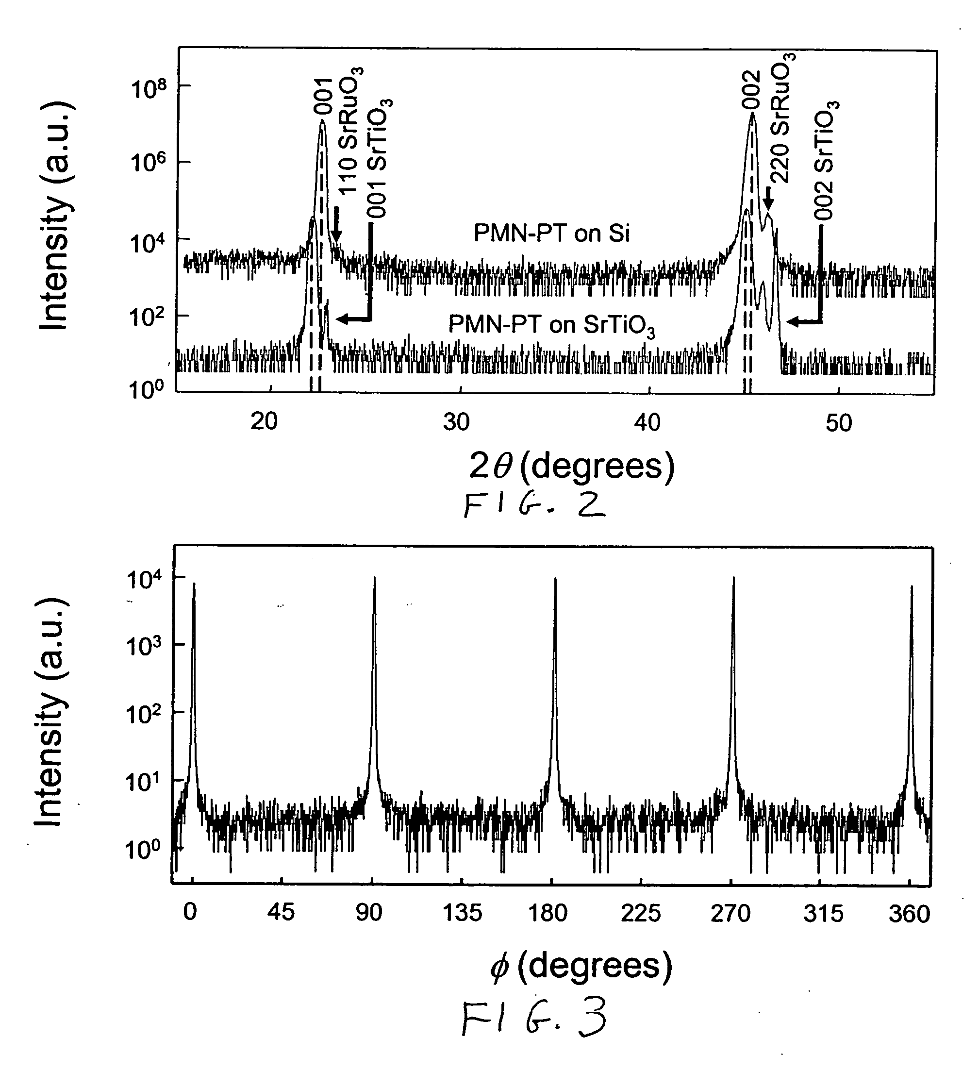
[0029] An example of a preferred substrate 21 that may be utilized in the invention is a (001) Si wafer coated with a seed layer 24 of SrTiO3. The epitaxial SrTiO3 layer 24 may be deposited by reactive molecular beam epitaxy (MBE) or other suitable processes. A suitable process is described in J. Lettieri, “Critical Issues of Complex, Epitaxial Oxide Growth and Integration with Silicon by Molecular Beam Epitaxy,” Ph.D. Thesis (Pennsylvania State University, 2002), available on-line at http: / / etda.libraries.psu.edu / theses / approved / WorldWidelndex / ETD-202 / index.html. The top surface 23 of the (001) Si wafer 21 is preferably miscut by 1° to 20°, most preferably 4°, toward (110) to improve the epitaxy of PMN-PT thick films and suppress pyrochlore phase formation. A 100 nm thick conducting SrRuO3 bottom electrode 26 is then deposited at a substrate temperature of 600° C. by 90° off-axis radio-frequency (RF) magnetron sputteri...

example 2

Fabrication of a PZT-Based Piezoelectric Thin Film Structure

[0037] High quality epitaxial PZT thick films up to 4 μm were fabricated on both (001) SrTiO3 and 4 degree miscut (001) Si substrates. Epitaxial (001) PZT films with various thicknesses (0.4-41 μm) were grown on (001) SrTiO3 and 4 degree miscut (001) Si substrates using on-axis radio-frequency (RF) magnetron sputtering. The nominal composition of the sputtering target was PZT (Zr / Ti=52 / 48). Molecular-Beam-Epitaxy (MBE) was used to fabricate 100 Å of epitaxial (001) SrTiO3 on the Si substrate as a seed layer in order to grow epitaxial PZT films. MBE methods of growing SrTiO3 layers are described in, G. Y. Yang, J. M. Finder, J. Wang, Z. L. Wang, Z. Yu, J. Ramdani, R. Droopad, K. W. Eisenbeiser, and R. Ramesh, J. Mater. Res. 17, 204 (2002), the entire disclosure of which is incorporated herein by reference. Prior to the PZT film deposition, an epitaxial SrRuO3 bottom electrode was deposited by 90° off-axis RF magnetron sputt...

example 3

Fabrication of a BiFeO3-Based Piezoelectric Thin Film Structure

[0041] A four layer structure including a 4 degree miscut Si substrate, a SrTiO3 seed layer, a first overlayer composed of SrRuO3 (100 nm thick) and a second overlayer composed of BiFeO3 was fabricated. The SrTiO3 seed layer and the SrRuO3 overlayer were grown on the Si substrate using the same methods described in Example 1, above. A 600 nm thick BiFeO3 film was then deposited by on-axis RF-magnetron sputtering from a stoichiometric sintered target. During BiFeO3 film deposition, the substrate temperature is maintained at 690° C. with argon and oxygen partial pressures of 240 mTorr and 160 mTorr, respectively.


PUM

PropertyMeasurementUnit
Thicknessaaaaaaaaaa
Thicknessaaaaaaaaaa
Thicknessaaaaaaaaaa

Abstract

A perovskite-based thin film structure includes a semiconductor substrate layer, such as a crystalline silicon layer, having a top surface cut at an angle to the (001) crystal plane of the crystalline silicon. A perovskite seed layer is epitaxially grown on the top surface of the substrate layer. An overlayer of perovskite material is epitaxially grown above the seed layer. In some embodiments the perovskite overlayer is a piezoelectric layer grown to a thickness of at least 0.5 μm and having a substantially pure perovskite crystal structure, preferably substantially free of pyrochlore phase, resulting in large improvements in piezoelectric characteristics as compared to conventional thin film piezoelectric materials.

Description

STATEMENT OF GOVERNMENT RIGHTS [0001] This invention was supported by the National Science Foundation (NSF) under grant numbers 0296021 and 0313764. The United States federal government has certain rights in this invention.FIELD OF THE INVENTION [0002] This invention pertains generally to the field of semiconductor and related device manufacturing and particularly to perovskite-based thin film structures. BACKGROUND OF THE INVENTION [0003] Most microelectromechanical systems (MEMS) are based on silicon or other semiconductors. It is desirable to be able to incorporate mechanical actuators and sensors with the MEMS semiconductor substrate in a manner which is compatible with processing of semiconductor substrates to form microelectronics or other devices. Piezoelectric materials have been incorporated on substrates with MEMS devices to form various types of actuators, positioners, drivers, and sensing elements. Typically, this has been accomplished by producing piezoelectric elements...

Claims


Application Information

Patent Timeline
IPC IPC(8): B32B9/00B32B19/00B32B13/04C30B23/00C30B28/14C30B25/00C30B28/12
CPCC30B29/22C30B23/02H10N30/10516H10N30/8548H10N30/8561H10N30/079
Inventor EOM, CHANG-BEOMSCHLOM, DARRELL GALEN
Owner PENN STATE RES FOUND
Why Eureka
Try Eureka