Insulated gate type semiconductor device and manufacturing method thereof

a technology of semiconductor devices and manufacturing methods, applied in semiconductor devices, basic electric elements, electrical appliances, etc., can solve the problems of large number of manufacturing processes, and high device characteristics and reliability, and achieve the effect of lowering reliability, high design flexibility of auxiliary floating regions, and reducing the maximum peak valu

Active Publication Date: 2006-12-28
TOYOTA JIDOSHA KK +1
View PDF12 Cites 83 Cited by
  • Summary
  • Abstract
  • Description
  • Claims
  • Application Information

AI Technical Summary

Benefits of technology

[0022] That is, the insulated gate type semiconductor device directed to another aspect of the present invention has an auxiliary floating region surrounded by a drift region. The auxiliary floating region can promote to get the drift region in OFF state depleted. Furthermore, the auxiliary floating region is arranged below an auxiliary trench section for the auxiliary floating region. Therefore, there is no need to consider positioning and size of a gate electrode. Accordingly, design flexibility of an auxiliary floating region is high. On the other hand, it is not always necessary to arrange a floating region at bottom of the trench section in which gate electrode is built. Therefore, as long as no ion implantation from the bottom, problems such as deterioration of device characteristics and lowering of reliability do not occur.
[0023] It is preferable that the inventive insulated gate type semiconductor device further comprises an auxiliary intermediate floating region arranged further above top of the auxiliary floating region with being surrounded by the drift region, the auxiliary intermediate floating region corresponding to a first conduction type semiconductor, wherein the auxiliary trench section penetrates the auxiliary intermediate floating region, and top of the deposited insulating layer is arranged further above top of the auxiliary intermediate floating region. Thereby, peaks of electric field can be formed at three portions, at least, and a maximum peak value can be lowered. Accordingly, both higher withstand voltage design and lower on-resistance design can be realized.

Problems solved by technology

However, the semiconductor device of FIG. 30 has had the following problems.
Accordingly, in case the gate dielectric 24 is kept being formed with the gate trench 21 damaged, device characteristics and reliability are likely to lower.
As a result, on-resistance becomes large.
Therefore, the number of manufacturing process is larger and it takes time to complete.
Furthermore, since heat load is large, impurity of an N− drift region 12 (epitaxial layer) diffuses and impurity concentration becomes uneven.

Method used


Image

  • Insulated gate type semiconductor device and manufacturing method thereof
  • Insulated gate type semiconductor device and manufacturing method thereof
  • Insulated gate type semiconductor device and manufacturing method thereof

Examples


first embodiment

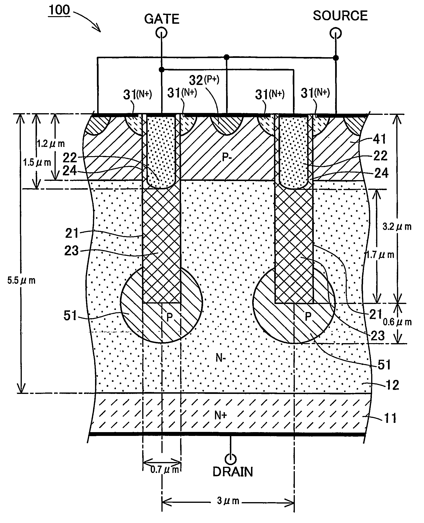
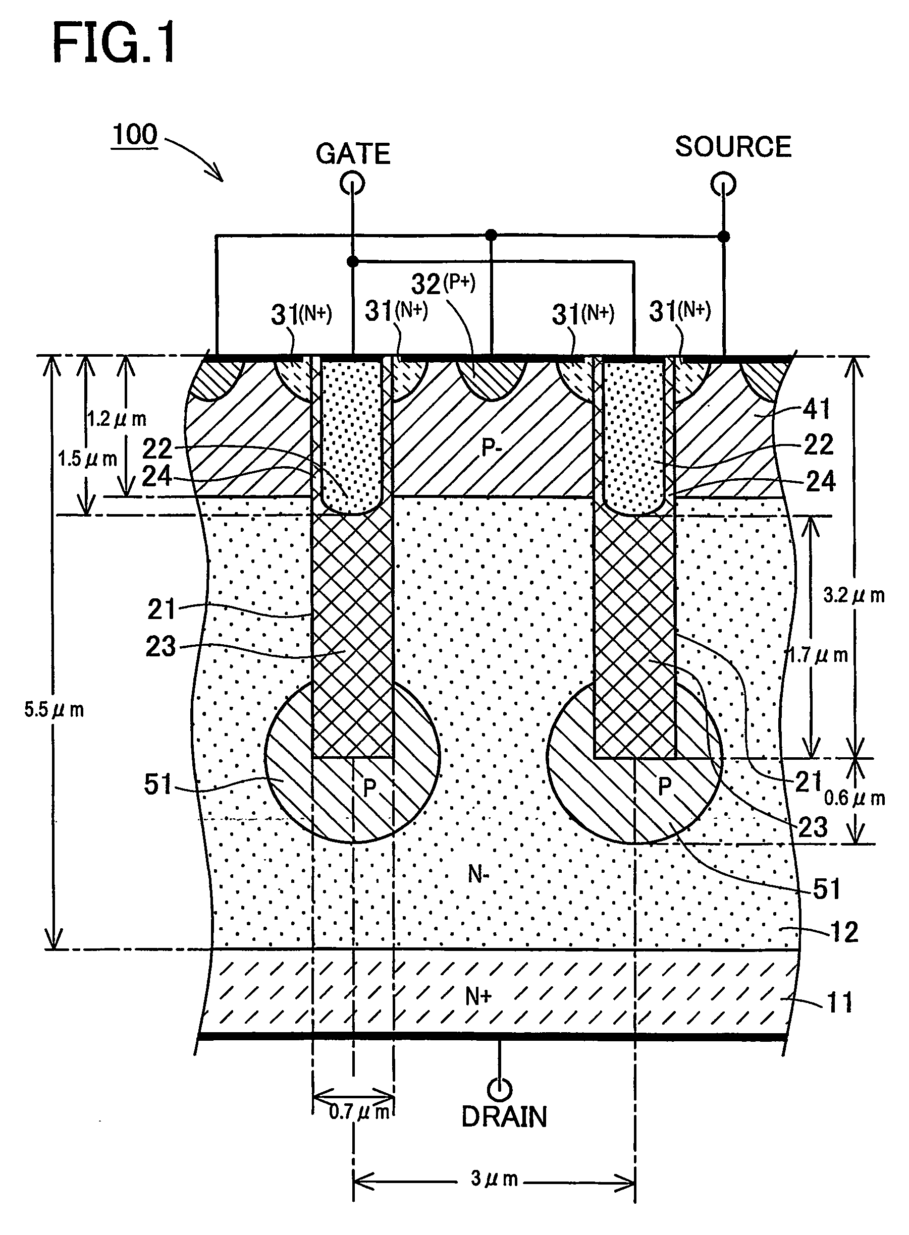
[0067] An insulated gate type semiconductor device 100 (hereinafter called semiconductor device 100) in a first embodiment has a structure as shown in a sectional view in FIG. 1. In FIG. 1, constituent elements having same reference numerals as in the conventional semiconductor device shown in FIG. 30 have same functions. In the present specification, the entire assembly formed by a start substrate and a single crystal silicon portion formed on the start substrate by epitaxial growth is called a semiconductor substrate.

[0068] In the semiconductor device 100, at the upper side in FIG. 1 in the semiconductor substrate, N+ source region 31 is formed together with P+ source region 32 provided at high concentration for lowering the contact resistance. At the lower side, on the other hand, N+ drain region 11 is provided. Between them, P− body region 41 and N− drift region 12 are provided from the upper side. The thickness of the combined region of P− body region 41 and N− drift region 12...

second embodiment

[0083] An insulated gate type semiconductor device 200 (hereinafter called semiconductor device 200) in a second embodiment has a structure as shown in a sectional view in FIG. 7. It is a feature of the semiconductor device 200 in this embodiment is that a trench for P floating region is provided, with the bottom of the trench positioned in the P floating region. In this respect, it is different from the semiconductor device 100 (see FIG. 1) in which the bottom of the trench incorporating the gate electrode is positioned in the P floating region. In FIG. 7, constituent elements having same reference numerals as in the semiconductor device 100 shown in FIG. 1 have same functions.

[0084] The semiconductor device 200, same as the semiconductor device 100 of the first embodiment, comprises N+ source region 31, N+ drain region 11, P− body region 41, and N− drift region 12. By excavating part of the upper side of the semiconductor device 200, a gate trench 21 is formed. The gate trench 21...

third embodiment

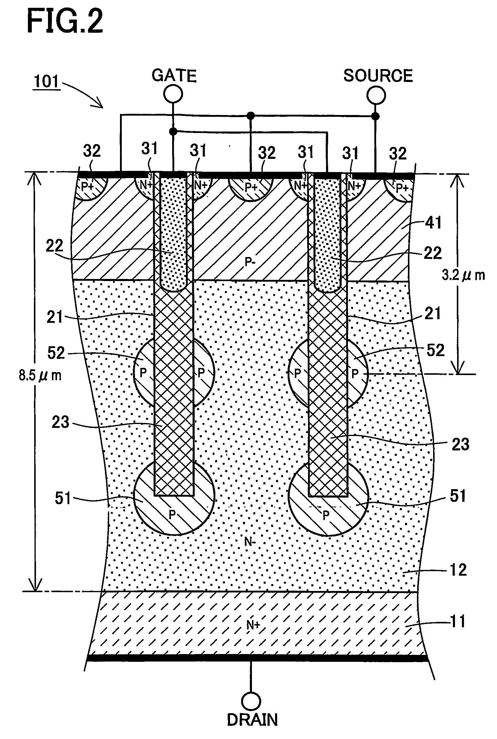
[0092] An insulated gate type semiconductor device 300 (hereinafter called semiconductor device 300) in a third embodiment has a structure as shown in a sectional view in FIG. 13. It is a feature of the semiconductor device 300 in this embodiment is that the P floating region is provided individually beneath a trench for gate electrode, and a trench for P floating region, that is, trench not incorporating the gate electrode. In this respect, it is different from the semiconductor device 100 (see FIG. 1) having the P floating region provided only beneath the gate trench 21 for gate electrode, or the semiconductor device 200 (see FIG. 7) provided only beneath the trench 25 for P floating region. In FIG. 13, constituent elements having same reference numerals as in the semiconductor device 100 shown in FIG. 1 and the semiconductor device 200 shown in FIG. 7 have same functions The semiconductor device 300, same as the semiconductor device 100 of the first embodiment and the semiconduct...


PUM


Abstract

The invention is intended to present an insulated gate type semiconductor device that can be manufactured easily and its manufacturing method while realizing both higher withstand voltage design and lower on-resistance design. The semiconductor device comprises N+ source region 31, N+ drain region 11, P− body region 41, and N− drift region 12. By excavating part of the upper side of the semiconductor device, a gate trench 21 is formed. The gate trench 21 floating region 51 is provided beneath the gate trench 21. A further trench 35 differing in depth from the gate trench 21 may be formed, a P floating region 54 being provided beneath the trench 25.

Description

TECHNICAL FIELD [0001] The present invention relates to an insulated gate type semiconductor device including trench gate structure and manufacturing method thereof. More particularly, it relates to an insulated gate type semiconductor device and manufacturing method thereof aiming to achieve both high withstand voltage design and low on-resistance design by relaxing electric field on semiconductor layer. BACKGROUND ART [0002] There have conventionally been proposed trench gate type semiconductor devices including trench gate structure as power device-dedicated insulated gate type semiconductor devices. For the conventional trench gate type semiconductor devices in general, high withstand voltage design and low on-resistance design are in trade-off relation. [0003] Patent Document 1, for example, discloses a trench gate type semiconductor device, which pays attention to the above trade-off relation. The trench gate type semiconductor device of Patent Document 1 has structure as sche...

Claims


Application Information

Patent Timeline
Patent Type & Authority Applications(United States)
IPC IPC(8): H01L29/94H01L21/336H01L29/06H01L29/08H01L29/423H01L29/739H01L29/78
CPCH01L29/0623H01L29/0634H01L29/0653H01L29/7813H01L29/42368H01L29/7397H01L29/7811H01L29/0834
Inventor TAKAYA, HIDEFUMIHAMADA, KIMIMORIKUROYANAGI, AKIRAOKURA, YASUSHITOKURA, NORIHITO
Owner TOYOTA JIDOSHA KK
Why Eureka
Try Eureka