Intergrated semiconductor memory and method for producing an integrated semiconductor memory

a technology of integrated semiconductor memory and semiconductor memory, which is applied in the direction of semiconductor devices, digital storage, instruments, etc., can solve the problems of high energy consumption of integrated semiconductor memory, temperature increases required for programming memory cells, and the inability to achieve temperature increases. , to achieve the effect of high current density

Inactive Publication Date: 2006-12-28
POLARIS INNOVATIONS
View PDF9 Cites 24 Cited by
  • Summary
  • Abstract
  • Description
  • Claims
  • Application Information

AI Technical Summary

Benefits of technology

[0030] One development of the invention provides for an electrically insulating layer to be deposited prior to the deposition of the material, and for the electrically insulating layer to be etched after the deposition of the material using the material as an etching mask. In this case, it increases the depth of the regions filled with material and...

Problems solved by technology

The higher the current required for changing the state of the storage medium and thus for rewriting the digital information, the higher the energy consumption of the integrated semiconductor memory.
Particularly in the case of phase change media and other storage media whose state is dependent on temperature, the currents for heating to the phase transition temperatures or melting points require a considerable amount of energy.
The temperature increases required for programming the memory cells can only be achieved by high programming currents.
Memory components comprising a phase change medium, which requires these high programmin...

Method used


Image

  • Intergrated semiconductor memory and method for producing an integrated semiconductor memory
  • Intergrated semiconductor memory and method for producing an integrated semiconductor memory
  • Intergrated semiconductor memory and method for producing an integrated semiconductor memory

Examples


Embodiment Construction

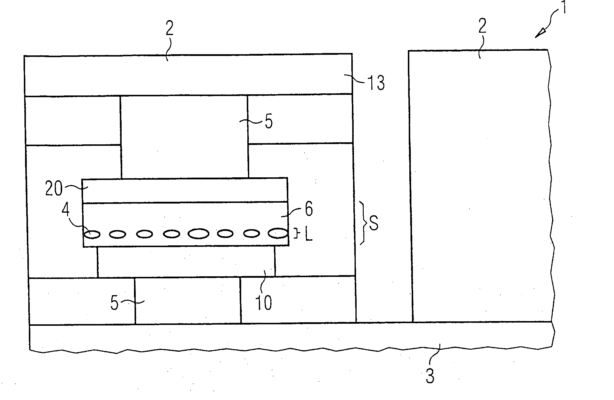
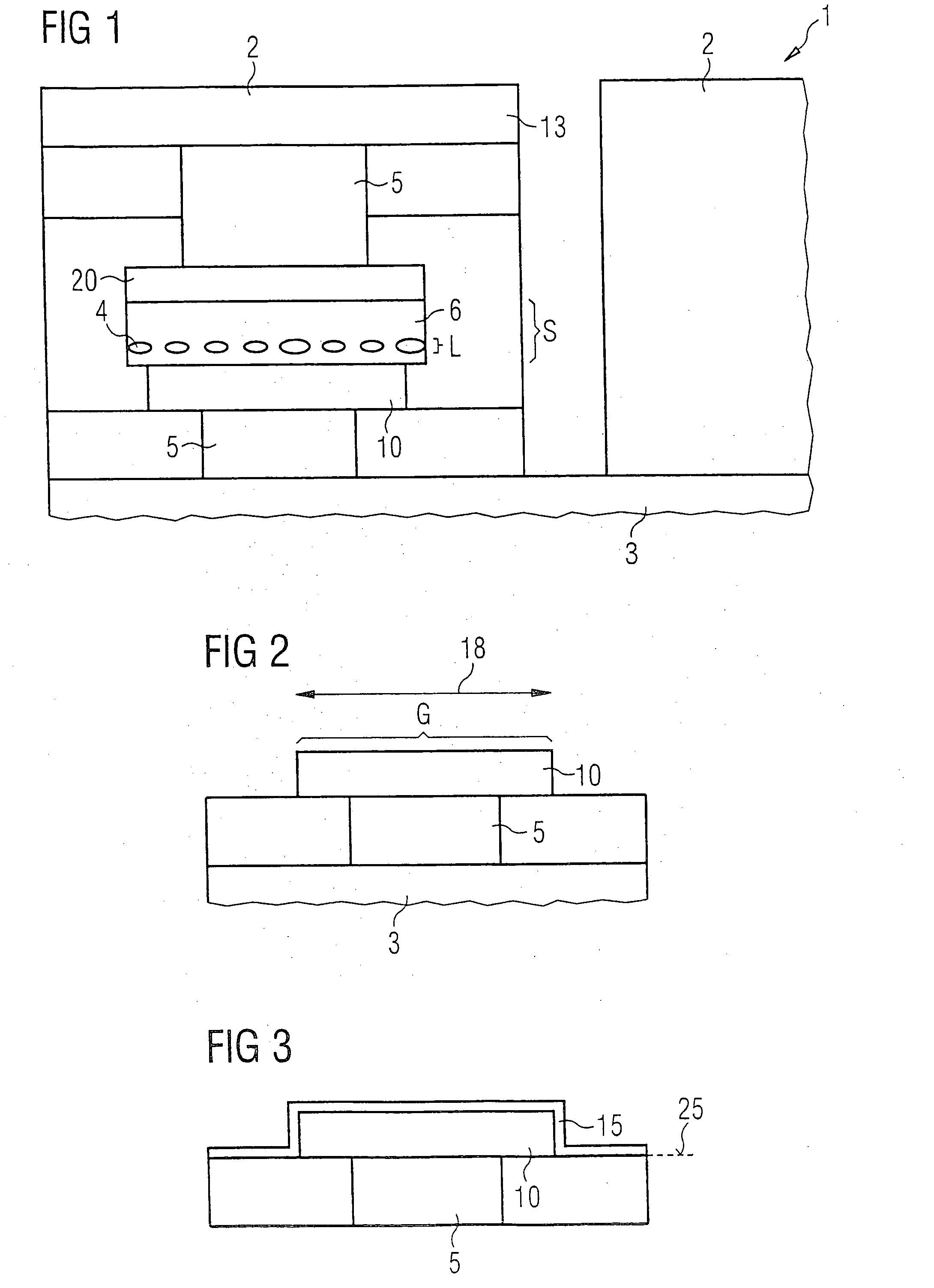
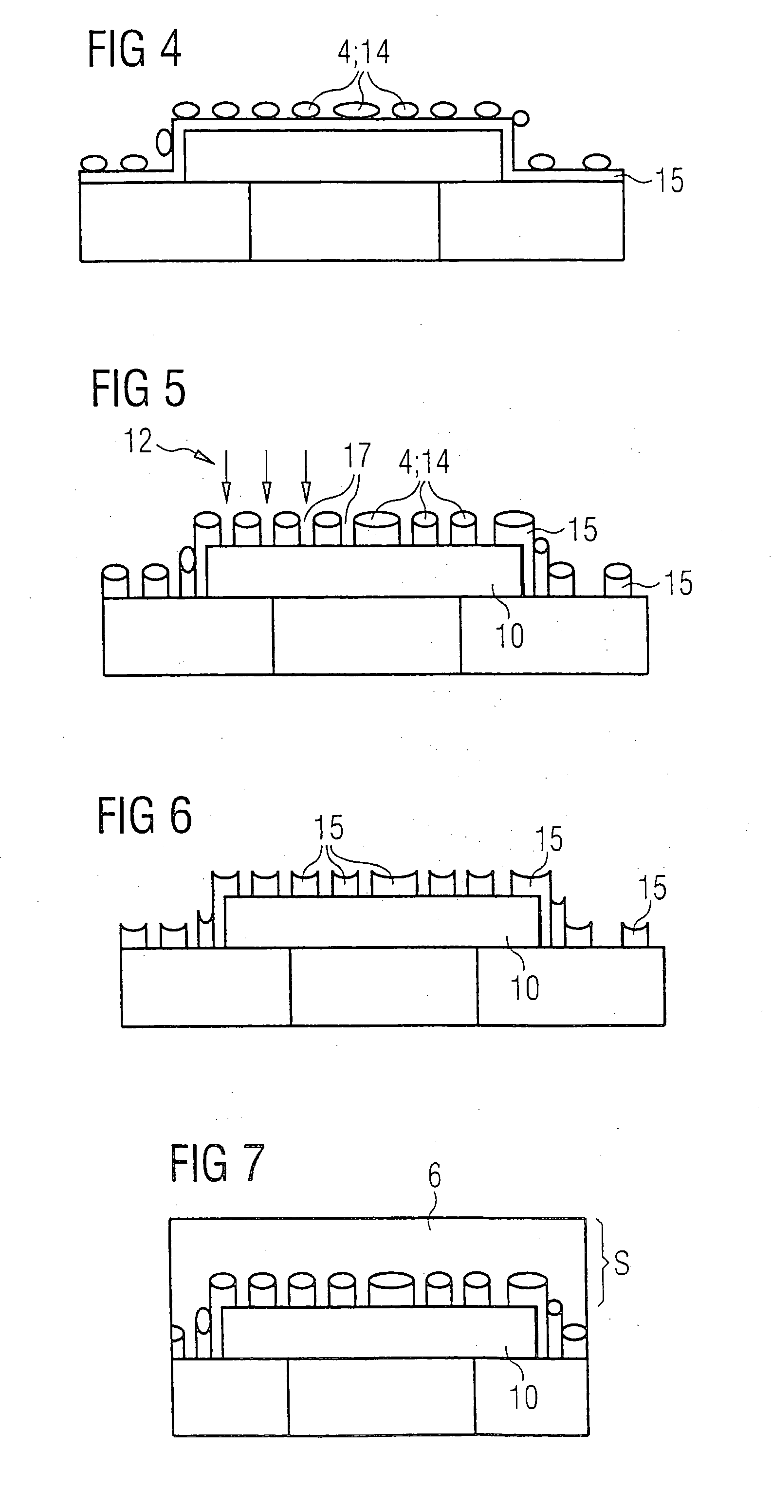
[0043]FIG. 1 shows a schematic cross-sectional view of a semiconductor memory 1 according to an embodiment of the invention, in which a memory cell 2, which is representative of the rest of the memory cells, has a first electrode 10, a second electrode 20 and a storage medium 6 in between. The electrodes 10, 20 are connected by contact connections 5 to corresponding interconnects or to the substrate 3 and an interconnect 13 situated at a higher level. In the lateral direction, the memory cell is shielded from adjacent memory cells by corresponding insulations.

[0044] According to embodiments of the invention, within the storage medium 6 provision is made of a layer or layer plane in which impurity particles made from a material 4 are incorporated, as a result of which, at the level of the layer plane, that proportion of the basic area of the storage layer situated between the electrodes 10, 20, which is covered with the storage medium 6 is reduced to a fraction or in any event to a ...


PUM


Abstract

An integrated semiconductor memory includes a storage medium (6) arranged between two electrodes (10, 20), which storage medium may be a phase change medium, for example. The storage medium (6) can be put into a first state or a second state by means of an electric current, as a result of which an item of information can be stored. According to embodiments of the invention, a layer plane (L) is provided in which impurity particles made from a material (4) are embedded, as a result of which the current density in the storage medium is locally increased and the programming current required for reprogramming is reduced. As a result, the current consumption of memory elements containing a phase change medium is reduced, so that for the first time they can be embodied with minimal feature size, together with other components such as transistors, and integrated into a single semiconductor circuit and no longer have to be arranged in separate subcircuits.

Description

[0001] This application is a continuation of co-pending International Application No. PCT / DE2004 / 002620, filed Nov. 25, 2004, which designated the United States and was not published in English, and which is based on German Application No. 103 56 285.0 filed Nov. 28, 2003, both of which applications are incorporated herein by reference.TECHNICAL FIELD [0002] The invention relates to an integrated semiconductor memory and to a method for producing an integrated semiconductor memory. BACKGROUND [0003] In semiconductor fabrication, semiconductor memories are produced that have a multiplicity of memory cells arranged in a memory cell array. A distinction is made between volatile and nonvolatile semiconductor memories. Nonvolatile semiconductor memories, which store stored information items even after the voltage supply has been turned off, may be formed as phase change memories. Phase change memories have a storage medium, which can assume two different states of different levels of ele...

Claims


Application Information

Patent Timeline
IPC IPC(8): G11C17/00H01L27/24H01L45/00
CPCH01L45/1246H01L45/1666H01L45/144H01L45/1233H01L45/06H10N70/828H10N70/231H10N70/061H10N70/8828H10N70/826G11C13/0004
Inventor HAPP, THOMAS D.PINNOW, CAY-UWESYMANCZYK, RALFUFERT, KLAUS-DIETER
Owner POLARIS INNOVATIONS
Why Eureka
Try Eureka