Molecular structures for gas sensing and devices and methods therewith

a gas sensor and molecular structure technology, applied in the field of molecular structures, can solve the problems of inconvenient device use, cumbersome, time-consuming, etc., and achieve the effects of reducing the cost of gas sensors, and improving the sensing efficiency

Inactive Publication Date: 2006-12-28
GENERAL ELECTRIC CO
View PDF7 Cites 56 Cited by
  • Summary
  • Abstract
  • Description
  • Claims
  • Application Information

AI Technical Summary

Benefits of technology

[0009] Accordingly, one aspect of the invention is a porous nanozeolite material having a first dimension less than about 1 micron and a second dimension less than about 100 microns. The nanozeolite material comprises pores having an average diameter less than about 50 nm.

Problems solved by technology

Many gas sensors in the art have problems associated with interference, when more than one gas needs to be detected.
In miniaturized sensors, the area available for sensing is limited.
The challenges associated with implementing zeolites in sensing applications are generally related to synthesizing zeolites with sub-micron or nano morphologies, and to coating sensor devices with such materials without detrimental effects to the devices.
Such processes typically require high pressures, high temperatures, and long hydrolysis time, rendering them cumbersome, time consuming and not device friendly.
Also, the structure of zeolites formed by these processes is often difficult to control and is dictated by the reactants used, by the synthesis conditions such as temperature, time, and pH, and in particular, by the structure-directing agent used.
But such methods are typically incompatible with conventional semiconductor device fabrication processes and cannot typically be used without deleterious effects on device integrity.
Scalability of such processes for sensor production can also prove to be very challenging.

Method used


Image

  • Molecular structures for gas sensing and devices and methods therewith
  • Molecular structures for gas sensing and devices and methods therewith
  • Molecular structures for gas sensing and devices and methods therewith

Examples


example 1

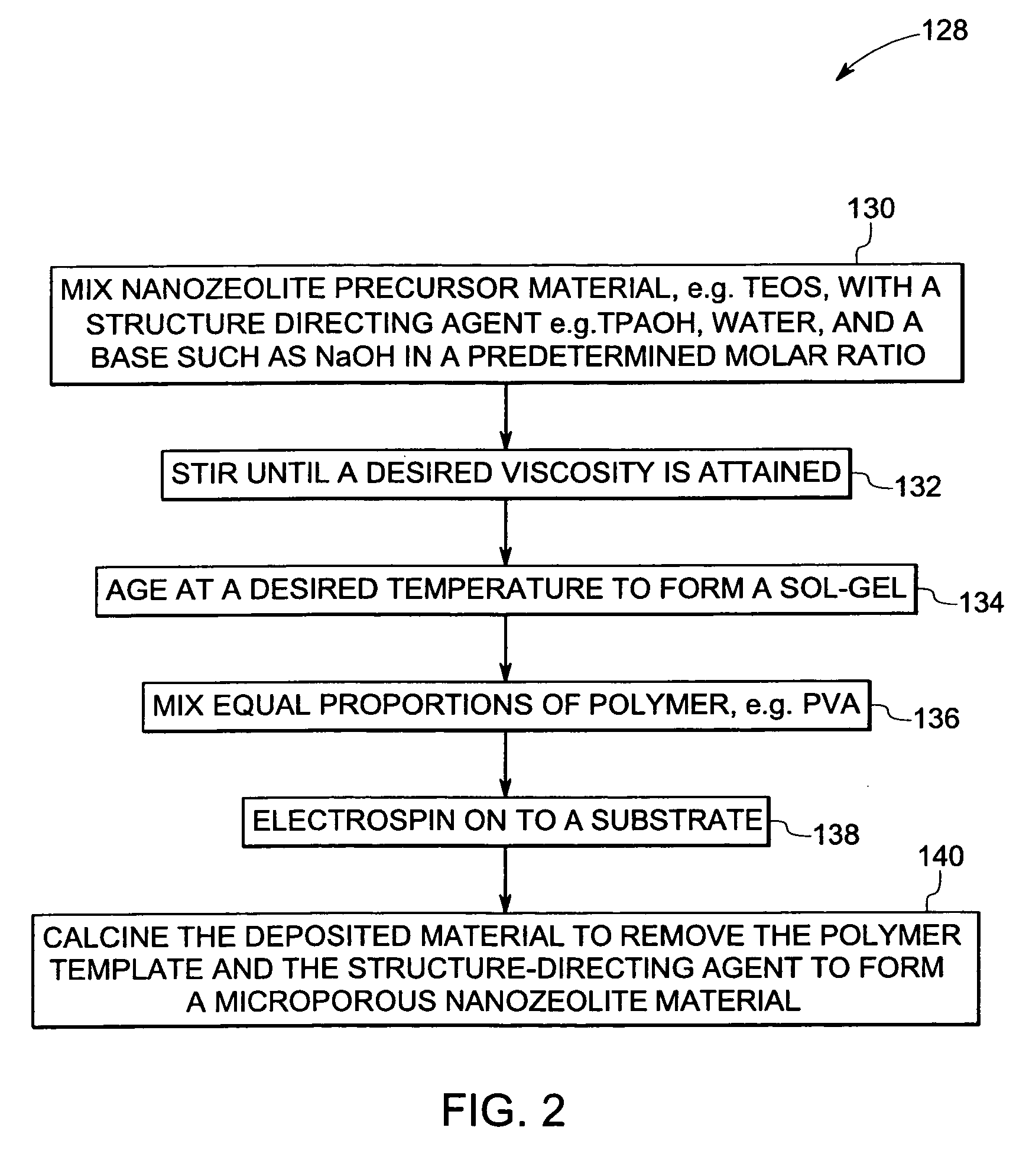
[0051] TEOS was mixed with a structure directing agent TPAOH, water, and NaOH, in a molar ratio of about 0.25:0.09:4.8:1.0. The mixture was subsequently stirred for about 4 to about 5 hours and aged at 70° C. for about 3 to about 6 hours resulting in a sol-gel. The resulting sol-gel was mixed in equal proportions with polyvinyl alcohol (PVA) and was used to electrospin the sol-gel and polymer solution directly on to a semiconductor substrate. The spinning distance was 15 cm and the applied voltage was 15 kV. After electrospun material deposited on the substrate is calcined at 500° C. for about 4 hours, to remove the polymer template and structure-directing agent to give a microporous nanozeolite material. FIG. 6 shows the scanning electron microscope (SEM) image of the microporous zeolites showing hybrid morphology 178. PVA enables the formation of needle-like structures 180.

example 2

[0052] TEOS was mixed with a structure directing agent TPAOH, water and NaOH in the molar ratio of about 0.25:0.09:4.8:1.0. The mixture was subsequently stirred for about 4 to 5 hrs and aged at 70° C. for 48 to 72 hours to form silicalite-1 zeolites. The synthesized silicalite-1 is powdered and calcined at 500° C. for about 4 hours to remove the structure directing agent. The powdered silicalite-1 particles are mixed with polyvinyl alcohol (PVA) to give it the required viscosity for spinning and electrospun to form microporous silicalite-1 nanozeolite. FIG.7 is a SEM micrograph showing microporous silicalite-1 with PVA after electrospinning. Silicalite-1 particles 184 of varied diameters can be seen embedded in polymeric fibers 182. The zeolite particle size can be controlled in the nanometer range to help enhance the active surface area of the sensing material and to help increase gas adsorption capability.

example 3

[0053] A sol-gel aqueous solution consisting of TEOS or tetra methyl orthosilicate (TMOS) with structure directing agent cetyltrimethylammonium bromide (CTAB) was used to synthesize mesoporous nanozeolite. The molar ratio of TEOS:Water:CTAB was fixed at about 4:8:1. TEOS was first hydrolyzed in an acidic environment (pH=1.85) and the resultant precursor solution is added drop-wise to the structure directing agent solution (CTAB) and aged for about 36 to about 48 hrs. A Brooke Field Viscometer was used to measure the sol-gel solution viscosity as a function of time and pH. The solution was electrospun and calcined at a spinning distance of about 7 cm to about 15 cm. The electrospun material was calcined at 500° C. for about 2 hour to evaporate the structure-directing agent to give mesoporous MCM-41 type nanozeolites with diameters in the micron to nanometer range with high aspect ratios. FIGS. 8, 9, 10 and 11 are SEM micrographs of MCM-41 type mesoporous nanozeolite materials. The en...


PUM

PropertyMeasurementUnit
diameteraaaaaaaaaa
diameteraaaaaaaaaa
diameteraaaaaaaaaa

Abstract

A porous nanozeolite material having a first dimension less than about 1 micron and a second dimension less than about 100 microns. The nanozeolite material comprises pores having an average diameter less than about 50 nm. A method of making microporous nanozeolites is provided. The method comprises the steps of providing an aqueous solution comprising at least one nanozeolite precursor material or zeolite particles, and electrospinning the aqueous solution onto a substrate to form an electrospun material. The electrospun material comprises microporous nanozeolites. A method of making mesoporous nanozeolites is also provided. The method comprises the step of providing an aqueous solution comprising a nanozeolite precursor material and at least one structure directing agent, and electrospinning the aqueous solution onto a substrate to form an electrospun mesoporous nanozeolite material. A gas sensor device is provided. The device comprises nanozeolite sensing material.

Description

CROSS REFERENCE TO RELATED APPLICATIONS [0001] This application claims the benefit of U.S. Provisional Application No. 60 / 651,866 filed on Feb. 09, 2005, which is incorporated herein in its entirety by reference.BACKGROUND OF THE INVENTION [0002] The invention relates to molecular structures. Particularly, the invention relates to porous molecular structures. [0003] Multiple gas sensing requires materials with desirable selectivity and sensitivity to adsorbent gas molecules and volatile vapors. Many gas sensors in the art have problems associated with interference, when more than one gas needs to be detected. Additionally, filters or traps are needed to block gas molecules, which are not being sensed. [0004] Microporous and mesoporous zeolites, because of their highly porous framework along with tunable pore and channel dimensions, large active surface area, variable hydrophilic and hydroscopic nature, and electrostatic behavior, are potential materials for chemical and gas sensing ...

Claims


Application Information

Patent Timeline
Patent Type & Authority Applications(United States)
IPC IPC(8): B01J29/04H05F3/00
CPCB82Y15/00B82Y30/00D01F9/10D01D5/003C01B39/04
Inventor SRINIVASAN, DURAISWAMYZRIBI, ANISRAO, RASHMI RAGHAVENDRAVETRIVEL, RAJAPPAN
Owner GENERAL ELECTRIC CO
Why Eureka
Try Eureka