Production method of a capacitor

a production method and capacitor technology, applied in the field of capacitors, can solve the problems of inability to achieve good esr value, inability to successfully form semiconductor layers, and inability to increase the impergnation ratio within a normal time, and achieve good esr performance, good performance, and high capacitance

Active Publication Date: 2007-01-04
SHOWA DENKO KK
View PDF21 Cites 24 Cited by
  • Summary
  • Abstract
  • Description
  • Claims
  • Application Information

AI Technical Summary

Benefits of technology

[0075] The capacitor produced by the method of the present invention can be preferably used for circuits requiring a high-capacitance and low ESR capacitor, such as a central processing circuit and a power source circuit. These circuits can be used in various digital devices such as a personal computer, server, camera, game machi...

Problems solved by technology

According to the methods of Japanese Patent Nos. 1,985,056 and 2,826,341, good ESR may be obtained, but a long time is necessary to form a semiconductor layer and the impregnation ratio cannot be increased within a normal time.
The method of Japanese Patent No. 2,826,341 is disadvantageous in that counter electrodes are necessary for simultaneously forming semiconductor layers on multiple electric conductors in an industrial scale and the semiconductor layer attaches also to the counter electrodes.
Also, the methods of Japa...

Method used


Image

  • Production method of a capacitor
  • Production method of a capacitor
  • Production method of a capacitor

Examples


example 1

[0081] By using and shaping a tantalum powder having CV (product of capacitance and electrochemical voltage) of 150,000 μF·V / g together with a Ta lead wire of 0.24 mmφ, a sintered bodies in a size of 4.5×1.0×1.5 mm were produced (sintering temperature: 1,300° C., sintering time: 20 minutes, density of sintered body: 6.2 g / cm3; the Ta lead wire was vertically embedded in the center part of the 1.0×1.5 mm face of the sintered body while being buried 4 mm inside the sintered body and protruding 10 mm outside). On a separately prepared polyimide-made resin plate having a length of 250 mm, a width of 30 mm and a thickness of 2 mm (There are provided by printed wiring, on the front surface of the plate, a circuit connecting connection terminals for 32 electric conductors and respective anodes of current regulated diodes and reaching the power supply terminal in the left side of plate, and on the back surface, a circuit electrically connected only to the connection terminals for electric c...

example 2

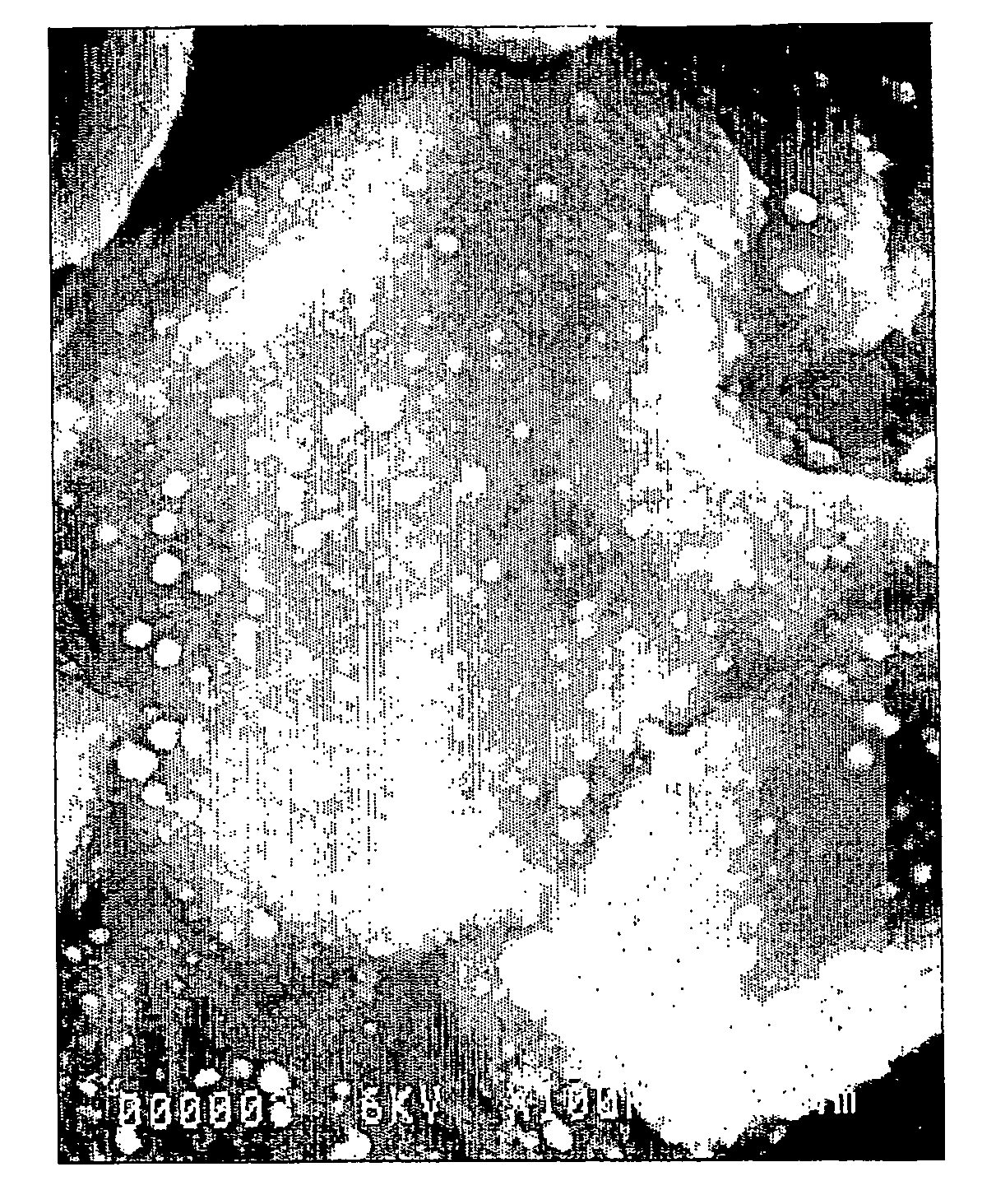
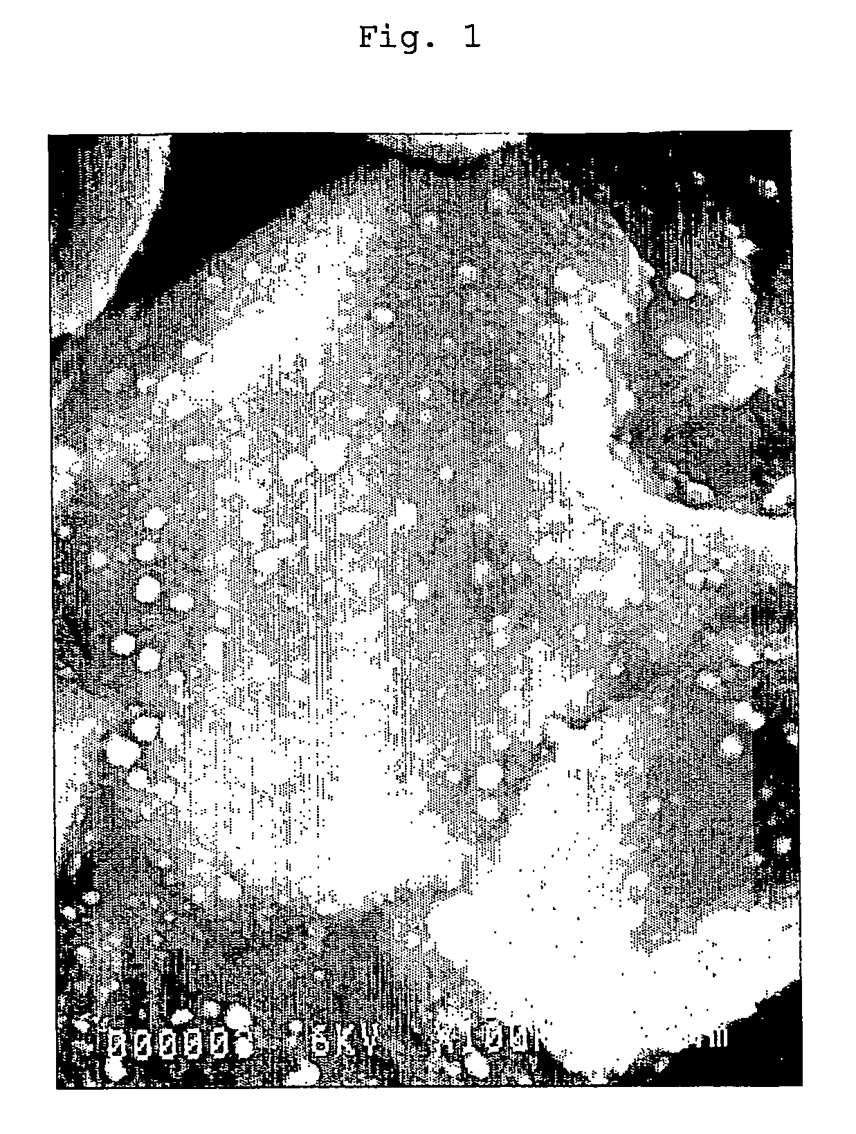
[0086] An oxide dielectric film layer comprising Nb2O5 was formed through electrochemical formation at 23 V by using a niobium sintered body (made of powder having CV of 270,000 μF·V / g, nitrided amount: 10,000 ppm, amount of oxygen due to natural oxidation on the surface: 84,000 ppm, sintering temperature: 1,280° C., sintering time: 30 minutes, density of the sintered body: 3.4 g / cm3) and a niobium lead wire in place of the tantalum sintered body and the tantalum lead wire in Example 1. Then, a series of operations, that is, the sintered bodies were dipped in an alcohol solution of 2% ethylenedioxythiophene, pulled up, left standing, dipped in an alcohol solution of 18% iron naphthalenesulfonate, pulled up, left standing at 40° C. for 30 minutes and dipped in alcohol, were repeated seven times, whereby fine protrusions mainly comprising ethylenedioxy polymer were produced on the dielectric layer. When observed through SEM, the fine protrusions had an island- or string-like shape wit...

example 3

[0088] Capacitors were produced in the same manner as in Example 1 except for producing the sintered body (sintering temperature: 1,360° C., sintering time: 20 minutes, density of the sintered body: 6.0 g / cm3) by using tantalum powder having a CV value of 70,000 μF·V / g in place of the tantalum powder used in Example 1.

[0089] The capacitance, impregnation ratio, ESR value and LC value of each of the capacitors produced above were measured by the following methods. The measurement results (average values) are shown in Table 1.

Capacitance of the Capacitor:

[0090] The capacitance was measured at room temperature and 120 Hz by using an LCR measuring meter manufactured by Hewlett Packard, Ltd.

Impregnation Ratio:

[0091] This is a percentage of a numerical value obtained by dividing the capacitance of the capacitor by the capacitance of each electric conductor having formed thereon a dielectric layer as measured in 30% sulfuric acid. ESR value:

[0092] The equivalent series resistance o...


PUM

PropertyMeasurementUnit
Fractionaaaaaaaaaa
Electrical conductivityaaaaaaaaaa
Lengthaaaaaaaaaa

Abstract

The present invention relates to a method for producing a capacitor comprising, as one electrode, an electric conductor having formed on the surface thereof a dielectric layer and, as the other electrode, a semiconductor layer formed on the electric conductor by energization using the electric conductor as the anode, wherein fine protrusions are formed on the dielectric layer before energization; a capacitor produced by the method thereof having a good capacitance appearance factor and a low ESR; and an electronic circuit and an electronic device using the capacitor.

Description

CROSS REFERENCE TO THE RELATED APPLICATIONS [0001] This is an application filed pursuant to 35 U.S.C. Section 111(a) with claiming the benefit of U.S. Provisional application Ser. No. 60 / 507,942 filed Oct. 3, 2003 under the provision of 35 U.S.C. Section 111(b), pursuant to 35 U.S.C. Section 119(e)(1).TECHNICAL FIELD [0002] The present invention relates to a capacitor having a good capacitance appearance factor and a low ESR. BACKGROUND ART [0003] A capacitor used in a circuit associated with the central processing unit (CPU) in personal computers and the like is required to have high capacitance and low ESR (equivalent series resistance) in order to prevent the fluctuation of voltage and reduce the generation of heat at the passing of a high ripple current. In general, an aluminum or tantalum solid electrolytic capacitor is used. [0004] The solid electrolytic capacitor is constituted by an aluminum foil having fine pores in the surface layer or a tantalum powder sintered body havin...

Claims


Application Information

Patent Timeline
IPC IPC(8): H01G9/00H01G9/15
CPCH01G9/0032H01G9/0036H01G9/042H01G9/07Y10T29/417H01G11/48H01G11/56Y02E60/13H01G9/15
Inventor NAITO, KAZUMI
Owner SHOWA DENKO KK
Why Eureka
Try Eureka