[0009] Conventional
metal-
oxide-semiconductor
field effect transistor (
MOSFET) designs face significant challenges as they are scaled down to improve cost and / or performance with each new generation of technology used to manufacture integrated circuits (ICs). In particular, the techniques used to reduce static
power consumption by minimizing source-to-drain leakage current (e.g., increased channel
doping, decreased gate-
dielectric thickness, and decreased source and drain junction depths) tend to also decrease transistor performance by decreasing on-current. By forming MOSFETs using a semiconductor substrate having precisely-formed and regularly-spaced stripes (ridges of semiconductor material(s)), both high performance (i.e., high on-current) and low static
power consumption (i.e., low source-to-drain leakage current) can be achieved. The stripes enable the formation of segmented channel regions that accommodate a wide range of gate-
electrode configuration options and also provide greater performance consistency between devices.
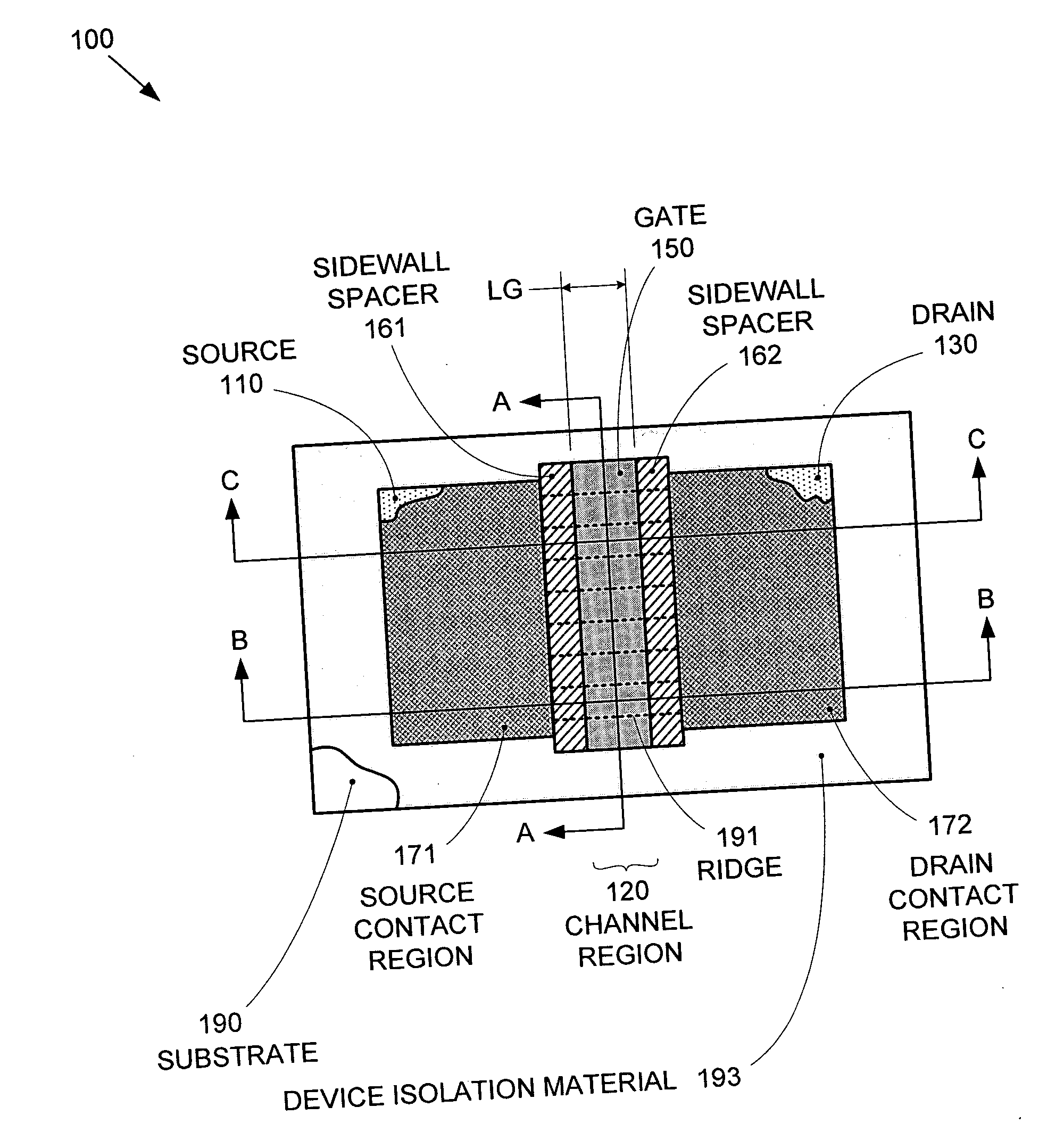
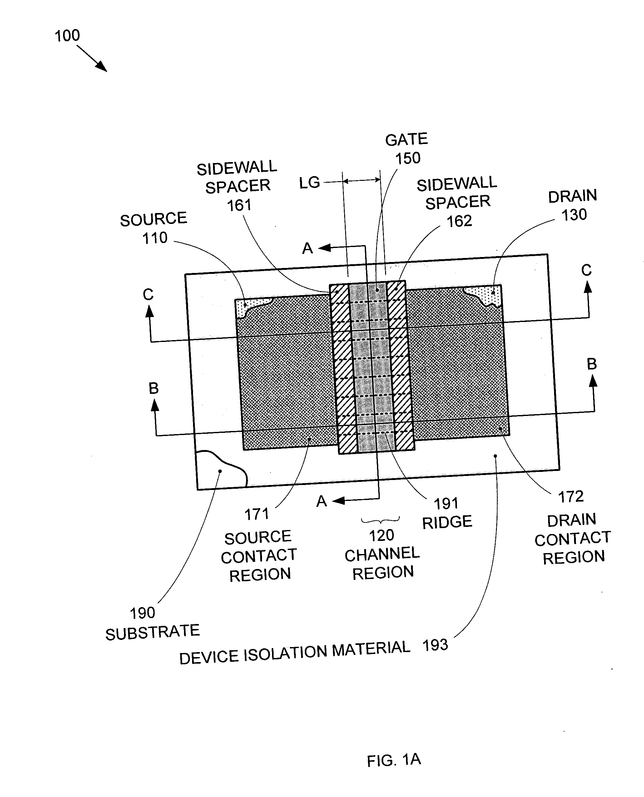
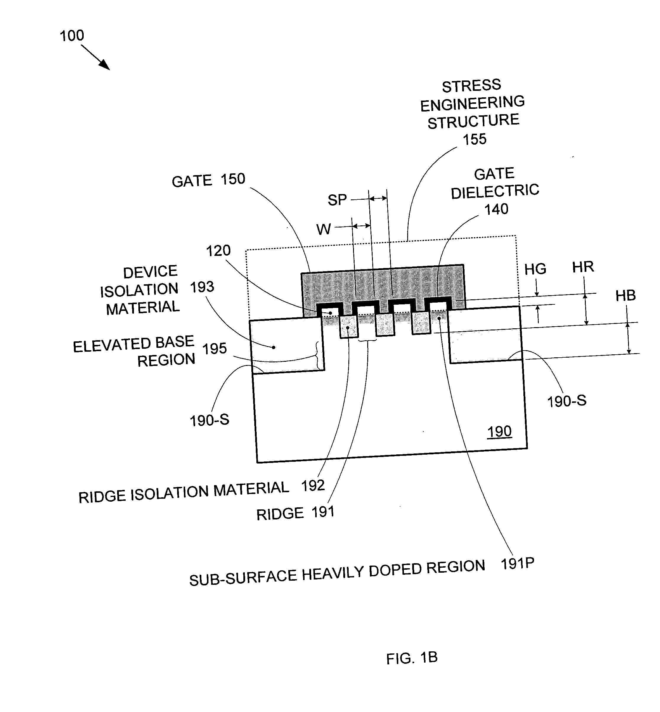
[0010] In one embodiment, a MOSFET can include a segmented channel region, in which one or more dimensionally precise
ridge(s) of semiconductor material (or materials) connect the source and drain regions. The ridges can themselves be formed on an elevated base region that extends a predetermined height above the adjacent substrate surfaces. An insulating material partially surrounds the
ridge(s), so that a top portion (“tip”) of each
ridge is exposed prior to the formation of the
gate stack (i.e. the gate-
dielectric and gate-
electrode layers). A gate
electrode (and interposing gate-
dielectric layer(s)) for each ridge is formed over the exposed tips of the ridges and “wraps” around those tips to provide enhanced control over source-to-drain leakage currents. (The gate electrode “straddles” the top portion of each ridge.) Heavily doped sub-surface regions within the ridges that begin at or near to the bottom of the tip (corresponding to the level of the insulating material) serve to further reduce source-to-drain leakage currents, thereby minimizing the static power consumption of the transistor. According to various other embodiments, any on-current enhancement or leakage-current reduction techniques applicable to conventional MOSFET constructions can also be applied.
[0011] In another embodiment, an IC (and method for producing the IC) incorporates multiple MOSFETs formed on pre-existing ridges on a corrugated substrate. Since the ridges on the corrugated substrate are geometrically very simple and very regular, high-precision fabrication techniques (e.g., imprint
lithography or spacer
lithography) can be used that would normally be impractical for actual device production. Once the corrugated substrate is available, the ridges on the substrate can be patterned based on the desired functional regions for the IC (i.e., by removing the ridges in the non-functional regions), and then forming an
insulation layer around and between the functional regions.
Gate dielectric layer(s)
and gate electrodes can then be formed over the ridges in the desired transistor locations, and various doping operations can be performed to define the source, drain, and channel regions for the MOSFETs. The IC formed in this manner will include MOSFETs having channel regions formed by one or more of the ridges, which helps to ensure that the MOSFETs exhibit accurate and consistent performance from
device to device. Adjacent MOSFETs in the IC (in the direction of the original ridges) can have precisely aligned channel region semiconductor segments, because those segments were originally formed from continuous ridges (i.e., the pre-existing ridges on the corrugated substrate). In various embodiments, the MOSFETs can include various source-to-drain
leakage current reduction techniques such as heavily doped sub-surface regions in channel regions and wrapped gates (i.e., gates that
wrap around the top portions of the ridges in the channel regions). In another embodiment, ridges in a pattern between two transistor locations can be filled in with
electrically conductive material to form an
electrical interconnect between the two transistor locations, thereby reducing metallization requirements.
[0012] A semiconductor
wafer can include one or more sets of precisely formed ridges, with each set of ridges including parallel ridges having the same height, width, and spacing. In one embodiment, the ridges in a single set of ridges can span the entire
wafer. In another embodiment, different sets of ridges can be formed at different locations on the
wafer. For example, each die region between scribe lines can have a particular arrangement of ridge sets, with ridges in different sets running in different directions to provide device fabrication flexibility.

