Mask, mask chip, manufacturing method of mask, manufacturing method of mask chip, and electronic device

a mask and manufacturing method technology, applied in the field of masks, can solve the problems of over-described metal masks, difficult to accurately manufacture such metal masks with a large size, and disadvantages, and achieve the effects of increasing the film thickness of a pixel, simplifying steps, and accurate patterning

Inactive Publication Date: 2007-01-25
SEIKO EPSON CORP
View PDF2 Cites 34 Cited by
  • Summary
  • Abstract
  • Description
  • Claims
  • Application Information

AI Technical Summary

Benefits of technology

[0011] An advantage of the present invention is to provide a mask and a mask chip that can be used for an accurate patterning of a large-size substrate on which film formation is performed, a manufacturing method of the mask, a manufacturing method of the mask chip, and an electronic device.
[0012] According to a first aspect of the present invention, a mask in which a plurality of mask chips are connected to one another via a supporting member includes a plurality of first opening sections that are provided in the plurality of mask chips and that correspond to a pattern to be formed; a cutout section provided at at least one of side faces opposing to each other of the mask chips adjacent to each other; a gap section is provided at a connected section connecting the mask chips adjacent to each other, the gap section is composed of the cutout section and includes a second opening section corresponding to a pattern to be formed; and a block section that is provided at least one of the mask chips adjacent to each other and that covers the gap section other than the second opening section.
[0013] According to the present invention, one mask is composed of a plurality of mask chips. Thus, such a mask can be easily provided that can form a thin film pattern larger than a mask chip (including a case where a plurality of thin film patterns are provided in a large area). For example, such a mask can be easily provided that can form a large thin film pattern as a constituting element of a display apparatus having a large-size screen.
[0014] By the way, when a plurality of mask chips are connected to a supporting member to form a pattern in a large-size substrate, an inconvenience has been caused where vapor deposition particles penetrate into a connected section having no pattern of mask chips adjacent to each other, causing an increased film thickness of a pixel at a part of the connection of the mask chips. In view of this, the inventor of the present application has conceived of a mask chip including a block section for blocking the connected section of the mask chips. According to the present invention, a clearance section having no pattern in the connected section of the mask chips adjacent to each other is blocked by the block section, thus blocking vapor deposition material by the block section. At the same time, vapor deposition material passes through a gap section at a pattern part in the connected section. This prevents vapor deposition material from penetrating into a part having no pattern of the connected section and thus prevents vapor deposition material from being formed at a part having no pattern. At the same time, other opening sections of the connected section effectively function as an opening section of one pattern. This can securely equalize thicknesses of all pixels, realizing a display apparatus having a further higher definition.
[0015] It is preferable that the block section is integrated with the mask chip.
[0016] According to this structure, a mask chip can be partially machined to form the block section. Thus, steps can be simplified. Furthermore, the continuous structure of the mask eliminates a junction between a mask chip and a block section. Thus, a mask having high strength can be provided.

Problems solved by technology

However, the above metal mask described in JP-A-2001-273976 has a disadvantage as described below.
However, it is very difficult to accurately manufacture such a metal mask that has a large size (large area) and that has a thin thickness.
This causes, when this metal mask is used to produce a large-size organic EL panel, an increase in a cumulative error value due to the thermal expansion.
Thus, the use of the metal mask has been limited to the manufacture of a small to medium size panel having a size of 20 inches at most.
However, when a silicon-based vapor deposition mask is used to form a light-emitting layer or the like of an organic EL device, the diameter of 300 millimeters of the silicon wafer as described above has caused a limitation on the manufacture of a vapor deposition mask adapted to a large-size screen.
By the way, when a plurality of mask chips are connected to a supporting member to form a pattern in a large-size substrate, an inconvenience has been caused where vapor deposition particles penetrate into a connected section having no pattern of mask chips adjacent to each other, causing an increased film thickness of a pixel at a part of the connection of the mask chips.

Method used


Image

  • Mask, mask chip, manufacturing method of mask, manufacturing method of mask chip, and electronic device
  • Mask, mask chip, manufacturing method of mask, manufacturing method of mask chip, and electronic device
  • Mask, mask chip, manufacturing method of mask, manufacturing method of mask chip, and electronic device

Examples


Embodiment Construction

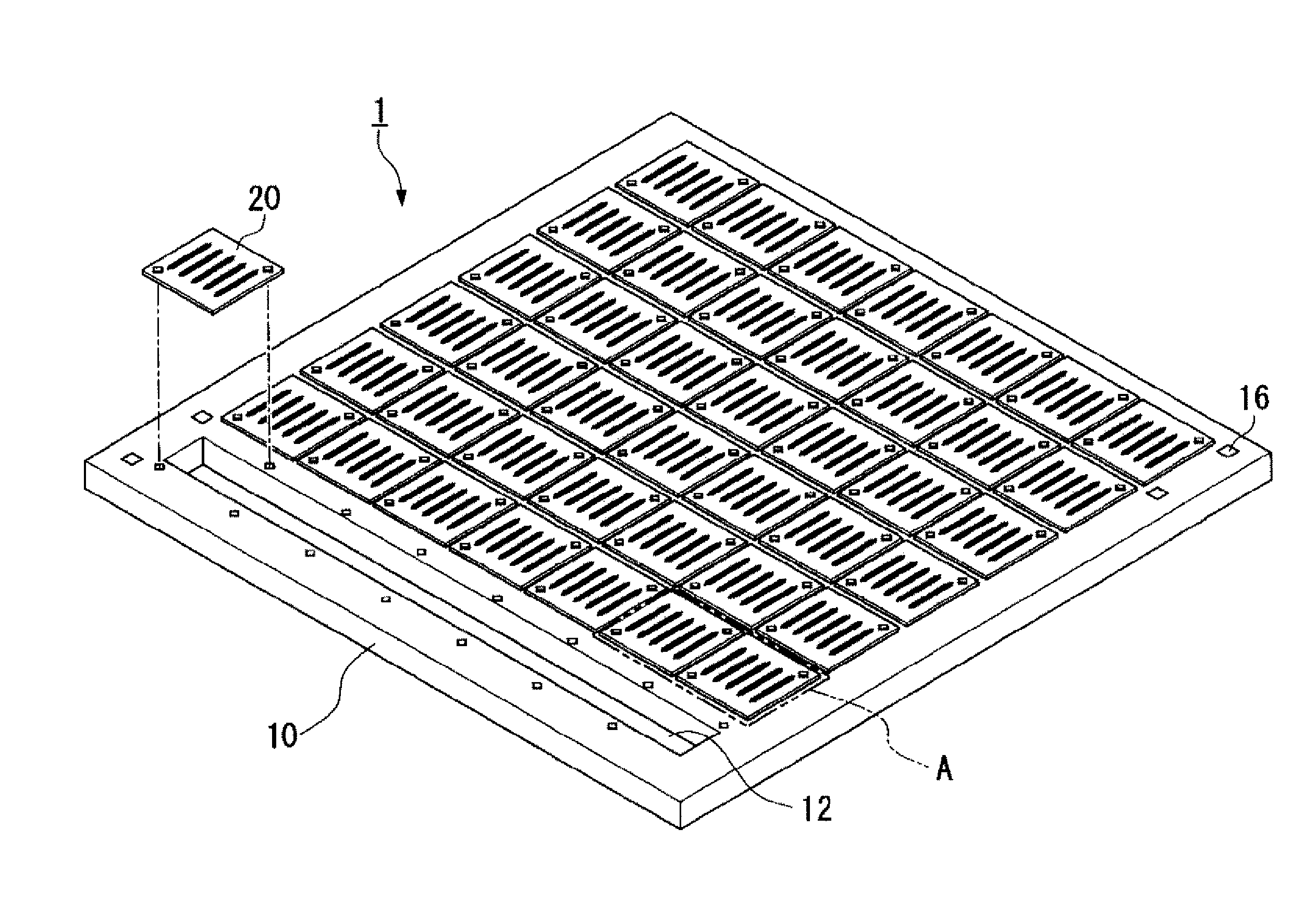
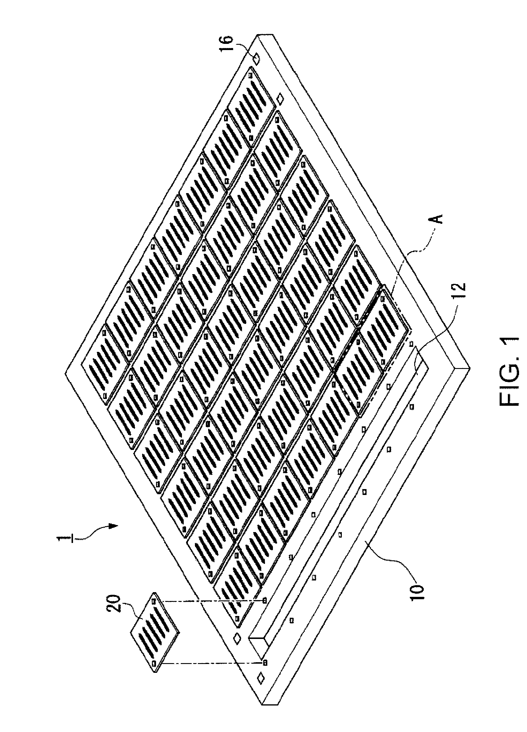
[0047] Hereinafter, embodiments of the present invention will be described with reference to the drawings. The respective drawings used in the following description show components appropriately scaled so that the respective components can be recognized. In this embodiment, a coordinate system in FIG. 1 is a right-hand x-y-z orthogonal coordinate system in which a Y-Z plane is parallel to the sheet of FIG. 1 and an X plane is vertical to a Y-Z plane.

[0048] (Structure of Mask)

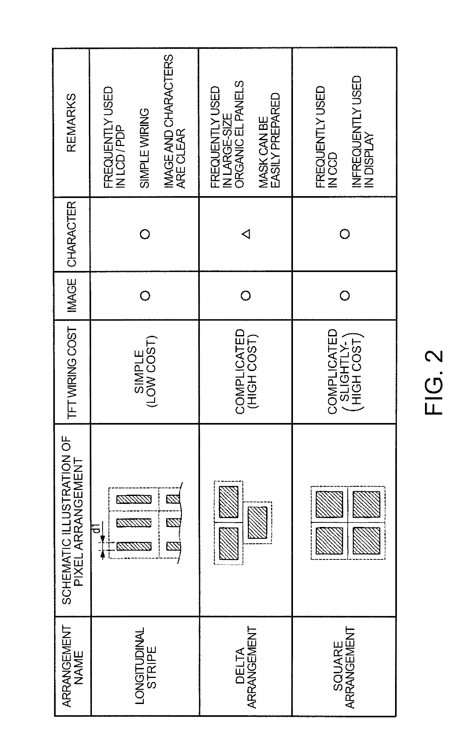
[0049]FIG. 1 is a perspective view schematically illustrating a mask. FIG. 2 illustrates an example of an arrangement of a pixel pattern formed by the mask shown in FIG. 1.

[0050] A mask 1 includes: a plurality of mask chips 20; and a glass substrate 10 (supporting member) to which the plurality of mask chips s 20 are adhered.

[0051] The mask chip 20 is made of silicon and is formed, as shown in FIG. 1, to include a plurality of long hole-shaped opening sections 22 (first opening sections) arranged to be paral...


PUM

PropertyMeasurementUnit
sizeaaaaaaaaaa
diameteraaaaaaaaaa
sizeaaaaaaaaaa

Abstract

A mask in which a plurality of mask chips are connected to one another via a supporting member, includes: a plurality of first opening sections that are provided in the plurality of mask chips and that correspond to a pattern to be formed; a cutout section provided at at least one of side faces opposing to each other of the mask chips adjacent to each other; a gap section provided at a connected section connecting the mask chips adjacent to each other, the gap section being composed of the cutout section and including a second opening section corresponding to a pattern to be formed; and a block section that is provided at at least one of the mask chips adjacent to each other and that covers the gap section other than the second opening section.

Description

BACKGROUND [0001] 1. Technical Field [0002] The present invention relates to a mask, a mask chip, a manufacturing method of the mask, a manufacturing method of the mask chip, and an electronic device. [0003] 2. Related Art [0004] An organic EL (electroluminescent) panel is composed of highly-responsive light emitting display elements in a layered structure of thin films. Thus, the organic EL panel has a light weight and can be used for a display apparatus providing a superior moving image. Thus, the organic EL panel recently has attracted much attention as a display panel for a flat panel display (FPD) television for example. A representative manufacturing method of the organic EL panel is disclosed in Appl, Phys, Lett, Vol. 51, No.12, p.p. 913-914, (1987). Specifically, the organic EL panel is manufactured in a manner as described below. A photolithographic technique is used to pattern a transparent anode (e.g., ITO (indium tin oxide)) to have a desired shape. Then, an organic mate...

Claims


Application Information

Patent Timeline
Patent Type & Authority Applications(United States)
IPC IPC(8): C23F1/00B44C1/22C03C25/68G02F1/1345
CPCG03F1/14C23C14/042G03F1/70H01L23/544H05B33/10G03F1/36H10K50/80
Inventor YOTSUYA, SHINICHIKUWAHARA, TAKAYUKIKOEDA, HIROSHI
Owner SEIKO EPSON CORP
Why Eureka
Try Eureka