Dielectric film production process and capacitor

a production process and dielectric film technology, applied in the direction of electrolytic capacitors, fixed capacitor details, fixed capacitors, etc., can solve the problems of oxidation and cease to function as electrodes, difficult to obtain dielectric films, and difficult to achieve dielectric films. achieve the effect of high dielectric constant, adequately inhibiting the oxidation of the metal layer, and high dielectric constan

Active Publication Date: 2007-02-01
TDK CORPARATION
View PDF5 Cites 11 Cited by
  • Summary
  • Abstract
  • Description
  • Claims
  • Application Information

AI Technical Summary

Benefits of technology

[0010] The dielectric film preferably consisting of particles with a mean particle size exceeding 40 nm. This will more notably exhibit the effect of the invention in terms of high dielectric constant and low leak current. The dielectric film more preferably consisting of particles with a mean particle size of less than 150 nm. This will yield an even more excellent capacitor, especially in terms of minimized leak current.
[0011] The dielectric film preferably contains at least one compound selected from the group consisting of barium titanate, strontium titanate and barium strontium titanate. Using such metal oxides can result in sufficiently high dielectric constant even when the dielectric film is a thin-film.
[0012] The dielectric film production process of the invention comprises a precursor layer-forming step in which a precursor layer containing a dielectric material is formed on a metal layer, and an annealing step in which the precursor layer is heated for crystallization of the dielectric material in the precursor layer to form a dielectric film, wherein during at least part of the annealing step, the precursor layer is heated to 550 to 1000° C. in a reduced pressure atmosphere with a pressure of 1×10⁻⁹ to 1×10³ Pa as measured with an ionization vacuum gage.
[0013] Heat treatment in an oxidizing atmosphere has conventionally been considered necessary to obtain high dielectric constant by heat treatment of dielectric materials such as metal oxides. According to the invention, however, the annealing step is carried out in a reduced pressure atmosphere with the pressure specified above, in order to allow production of a dielectric film capable of exhibiting sufficiently high dielectric constant, while adequately inhibiting oxidation of the metal layer. The present inventors conjecture that this effect is achieved by the production process of the invention because a dielectric film with density in the range specified above can be suitably obtained in a capacitor according to the invention.
[0014] The metal layer preferably includes at least one metal selected from the group consisting of Cu, Ni, Al, stainless steel and inconel. These metals, while being inexpensive, are readily oxidized, but according to the production process of the invention it is possible to obtain a dielectric film capable of exhibiting high dielectric constant while adequately inhibiting oxidation even when using such metals.
[0015] More preferably, the metal layer comprises Cu and the precursor layer is heated in the annealing step in a reduced pressure atmosphere with a pressure of 4×10⁻¹ to 8×10⁻¹ Pa as measured with an ionization vacuum gage. Alternatively and even more preferably, the metal layer comprises Ni and the precursor layer is heated in the annealing step in a reduced pressure atmosphere with a pressure of 2×10⁻³ to 8×101 Pa as measured with an ionization vacuum gage. This will allow formation of a high-dielectric-constant dielectric film in a more efficient manner while adequately inhibiting volatilization of the metal layer itself.

Problems solved by technology

Still, when readily oxidized metals such as Ni or Cu are used as electrodes, heat treatment in an oxidizing atmosphere has been problematic because it causes the metals to be oxidized and cease to function as electrodes.
Processes for forming dielectric films by heat treatment in reducing atmospheres containing hydrogen or carbon monoxide have been carried out in the conventional art, but it has not been possible to obtain dielectric films as thin-films with adequately high dielectric constant by these processes.
Another problem of capacitors employing conventional dielectric films is a large leak current.

Method used


Image

  • Dielectric film production process and capacitor
  • Dielectric film production process and capacitor
  • Dielectric film production process and capacitor

Examples


Embodiment Construction

[0018] Preferred embodiments of the invention will now be described in detail. However, it is to be understood that the invention is in no way limited to these embodiments.

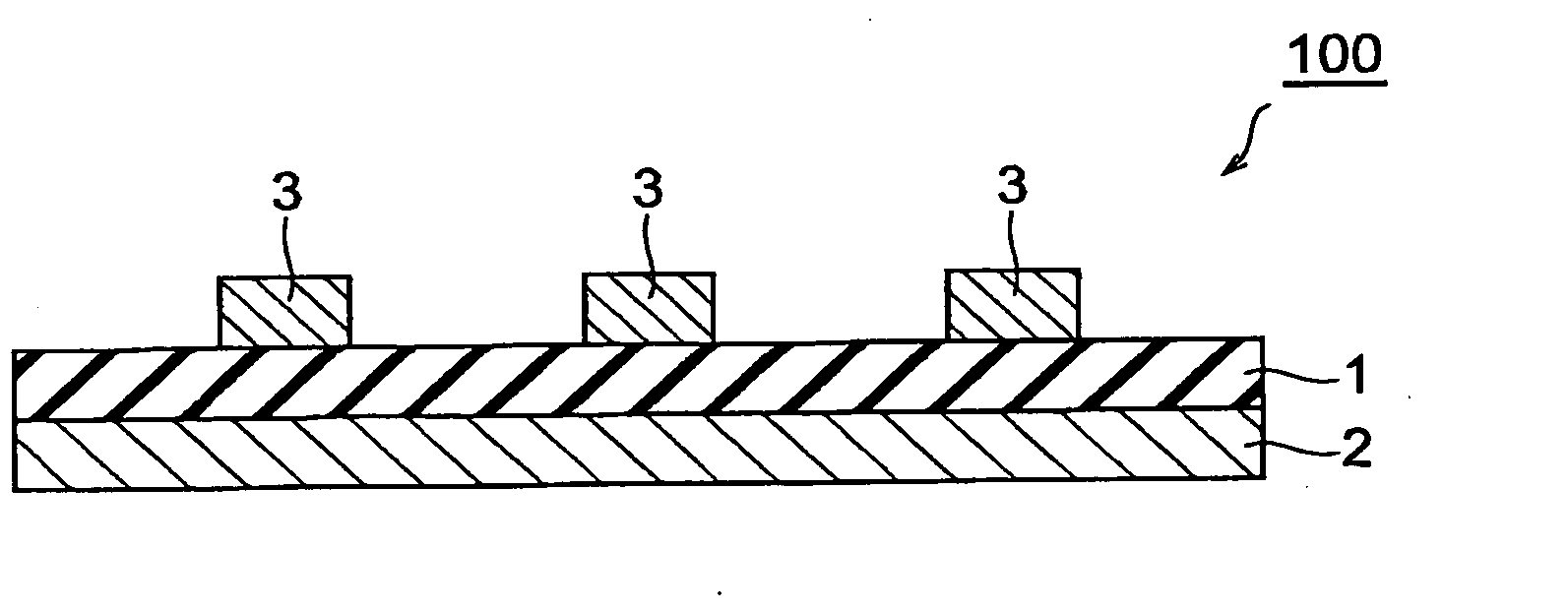
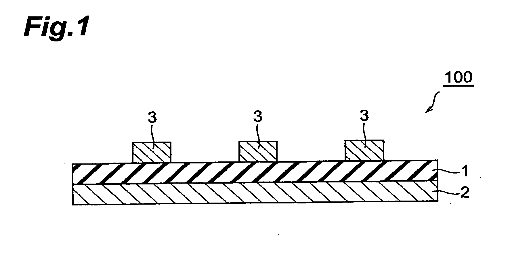
[0019]FIG. 1 is a cross-sectional view showing an embodiment of a capacitor according to the invention. The capacitor 100 shown in FIG. 1 is provided with a dielectric film 1, and a first electrode 2 and multiple second electrodes 3 formed sandwiching it and facing each other. A capacitor function is obtained at the sections where the first electrode 2 and the second electrodes 3 are facing.

[0020] The dielectric film 1 has a density exceeding 72% of the theoretical density calculated based on the lattice constant. The density of the dielectric film 1 is more preferably at least 80% and more preferably at least 85% of the theoretical density. The upper limit for this percentage is preferably as high as possible, and will usually be about 95%. The density of the dielectric film 1 may be determined, for example, by...


PUM

PropertyMeasurementUnit
mean particle sizeaaaaaaaaaa
particle sizeaaaaaaaaaa

Abstract

A capacitor provided with a dielectric film, and a first electrode and second electrode formed sandwiching it and facing each other, wherein the dielectric film has a density exceeding 72% of the theoretical density calculated based on the lattice constant, and either or both of said first electrode and said second electrode contain at least one metal selected from the group consisting of Cu, Ni, Al, stainless steel and inconel.

Description

BACKGROUND OF THE INVENTION [0001] 1. Field of the Invention [0002] The present invention relates to a dielectric film production process and a capacitor. [0003] 2. Related Background Art [0004] Active research has been conducted in recent years on thin-film capacitors that are provided with dielectric thin-films formed on Ni foils or Cu foils (Japanese Unexamined Patent Publication No. 2005-39282, and J. T. Dawley and P. G. Clem, Applied Physics Letters, 2002, Vol.81, No.16, p.3028). The dielectric materials that are primarily used for dielectric thin-films are metal oxide materials such as barium strontium titanate ((Ba,Sr)TiO3, abbreviated as “BST”) or lead zirconate titanate ((Pb,Zr)TiO3, abbreviated as “PZT”). These metal oxides are known to exhibit high dielectric constant after film formation or heat treatment in an oxidizing atmosphere. Increasing the dielectric constant can yield a capacitor with a large electrostatic capacity. SUMMARY OF THE INVENTION [0005] Still, when re...

Claims


Application Information

Patent Timeline
Patent Type & Authority Applications(United States)
IPC IPC(8): H01G4/06
CPCH01G4/1227H01L21/31691H05K2201/0355H05K1/162H05K2201/0175H01L27/016H01L21/02197H01G9/00H01L21/02356
Inventor UCHIDA, KIYOSHIHORINO, KENJISAITA, HITOSHI
Owner TDK CORPARATION
Why Eureka
Try Eureka