Unlock instant, AI-driven research and patent intelligence for your innovation.

Signal transmission method

a transmission method and signal technology, applied in the direction of electric variable regulation, process and machine control, instruments, etc., can solve the problems of requiring a larger wiring area, low noise withstanding capability, and hand held telephone sets and such electronic equipments, and achieve the effect of reducing the noise of the signal very effectively

Inactive Publication Date: 2007-02-08
FUJI ELECTRIC HLDG CO LTD
View PDF0 Cites 17 Cited by
  • Summary
  • Abstract
  • Description
  • Claims
  • Application Information

AI Technical Summary

Benefits of technology

[0049] The signal transmission method according to the invention superimposes a spread code onto an original signal (data to be transmitted) to synthesize a first signal, changes the switching frequency of a switching power supply based on the first signal to transmit the first signal to a plurality of semiconductor apparatuses (satellite apparatuses) via the output line of the switching power supply, and changes the output voltage level on the output line to transmit a second signal to the satellite apparatuses. By using the second signal for controlling and instructing the satellite apparatuses, the satellite apparatuses are shifted, for example, from the stopped state or the sand-by mode to the normal operation mode so that the satellite apparatuses may receive the first signal. Because the voltage level on the output line is monitored by a static means that does not employ any clock signal, the power consumption in the satellite apparatuses in the stopped state or in the sand-by mode is reduced. It is possible to omit the wiring for selecting the data to be transmitted and the satellite apparatus, to which the data is directed, in the same manner as the signal transmission method disclosed in the Patent Document 1. Because the data is transmitted in the form of ripples on the power supply bus and the period thereof is changed so that the ripple frequency may not be localized to a certain frequency, the EMI is reduced very effectively. Because the spread code is employed, data transmission quite immune to noises is realized.

Problems solved by technology

Accordingly, it is unavoidable that hand held telephone sets and such electronic equipments, in which more and more semiconductor apparatuses have been used, require a greater wiring area on the printed circuit board for the above described exclusive signal lines.
Furthermore, because these signals utilize a single frequency, the proposed interfaces are adversely affected easily by noises, causing a low noise withstanding capability.
Because the signal amplitude is the power supply voltage of the proposed interfaces, many radiated noise signals are generated, causing further hazards for down-sizing the hand held electronic equipments.
However, because it is necessary for the wire communication interface using the code division multiple access (CDMA) described in the Non-patent Document 1 to employ three communication lines including two data lines and one clock line, the wide wiring area problem has not been solved.
Although the data transmission method according to the invention disclosed in the Patent Document 1 has various specific features as described above, some problems remain unsolved if the current consumption thereof is considered.
Because the data transmission system disclosed in Japanese Patent Application Publication No. Hei. 4 (1992)-287598 (Paragraph , FIG. 2) changes the output voltage depending on the response of the power supply, it is impossible to realize high-speed communication.
If the level difference is small, the system is easily adversely affected by noise.
If the level difference is large, large EMI is caused.

Method used


Image

  • Signal transmission method
  • Signal transmission method
  • Signal transmission method

Examples


first embodiment

[0067] Although the block diagram showing the entire system configuration according to a first embodiment of the invention is the same as those illustrated in FIGS. 11 and 12, the configurations of the host and satellite apparatuses are different.

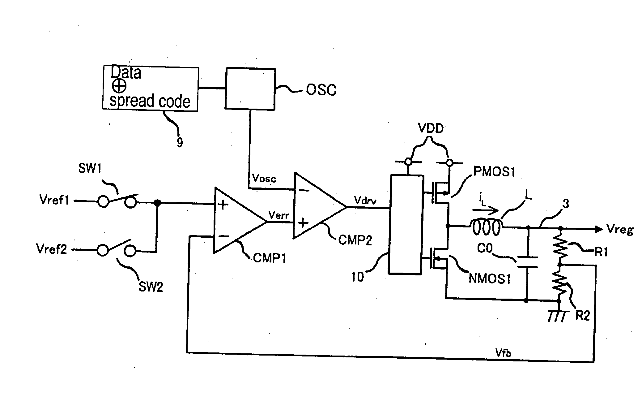
[0068]FIG. 1 is a block circuit diagram of a spread spectrum PWM DC / DC converter for the system described in FIGS. 11 and 12 and for the data transmission method according to the first embodiment of the invention. In FIG. 1, the same reference numerals and symbols as used in FIG. 13 are used to designate the same constituent elements and their duplicated descriptions are omitted for the sake of simplicity.

[0069] Referring to FIG. 1, the PWM DC / DC converter according to the first embodiment is different from the PWM DC / DC converter shown in FIG. 13 in that the non-inverting input terminal of comparator CMP1 in FIG. 1 is connected to reference voltages Vref1 and Vref1 via switches SW1 and SW2, respectively. Switches SW1 and SW2 are ON and O...

second embodiment

[0086] Because the signal transmission method according to the first embodiment is based on the use of the oscillator circuit described in FIG. 15, it is impossible for the signal transmission method according to the first embodiment to transmit two or more bits for one oscillation period of oscillator circuit OSC.

[0087] A signal transmission method according to a second embodiment that facilitates transmitting m bits every oscillation period of oscillator circuit OSC, is described below. The data to be transmitted is divided into data sections of m bits and the oscillation period of oscillator circuit OSC is determined by the m-bits data. FIG. 5 illustrates a circuit for generating an oscillation period in oscillator circuit OSC.

[0088] The circuit shown in FIG. 5 replaces the circuit block 40 surrounded by the broken lines in FIG. 15. In FIG. 5, the same reference numerals and symbols as used in FIG. 15 are used to designate the same constituent elements and their duplicated desc...

third embodiment

[0093]FIG. 6 is a block circuit diagram describing the configuration of a data transmission system according to a third embodiment of the invention. The circuit shown in FIG. 6, similar to that of FIG. 11, omits signal line 8, operable to transmit the synchronization signal. Because signal line 8 is omitted, the wiring area required for synchronization signal line 8 is unnecessary according to the third embodiment.

[0094] However, because the data transmission system according to the third embodiment is not provided with any synchronization signal line, it is necessary to include a synchronization supplementing circuit on the receiving side (cf. Non-patent Document 2), thereby increasing the circuitry, and therefore the area of circuit layout area, for the receiving side.

[0095] Although a tradeoff relation exists between the wiring area saved and the extra circuit layout area needed, the question of whether greater importance is attached to the wiring area or to the circuit layout ...


PUM


Abstract

A data transmission method superimposes a spread code onto data in order to synthesize a first signal. The method changes the switching frequency of a switching power supply based on the first signal, transmitting the second signal to a plurality of semiconductor apparatuses (satellite apparatuses) via an output line of the switching power supply. The method changes the DC output voltage level of the second signal on the output line of the switching power supply wherein a satellite apparatus may use the second signal for controlling and instructing the satellite apparatuses to make the satellite apparatus shift, for example, from the stopped state or the sand-by mode to the normal operation mode so that the satellite apparatus may receive the first signal.

Description

BACKGROUND OF THE INVENTION [0001] The present invention relates to a method for transmitting data to a semiconductor apparatus, the data operable to control the semiconductor apparatus. [0002]FIG. 8 is a block diagram of a system in which a host CPU 50 controls at least one semiconductor apparatus. Host CPU 50 further controls a switch 51 to supply the output from a battery 52 to a power supply line 53. Host CPU 50 communicates with another host CPU 55 and a subsidiary CPU 56 via a signal line 54. Host CPU 50 transmits control data to a DC / DC converter control IC 57, a liquid crystal driver control IC 58, a RAM 59, a display control IC 60 and such a semiconductor apparatus to control the operations of the semiconductor apparatuses. [0003]FIG. 9 is a block diagram of a system in which a power management controller 61 controls DC / DC converters. In FIG. 9, the same reference numerals as used in FIG. 8 are used to designate the same constituent elements and their duplicated explanation...

Claims


Application Information

Patent Timeline
IPC IPC(8): H04B1/00H02M3/155H04B3/54
CPCH02M3/156H04B14/026H04B1/707H02M2001/0025H02M1/0025
Inventor NISHIO, HARUHIKO
Owner FUJI ELECTRIC HLDG CO LTD