Adhesive film and image display device

a technology of adhesive film and adhesive layer, which is applied in the direction of film/foil adhesives, instruments, synthetic resin layered products, etc., can solve the problems of disturbing the liquid crystal order and images, difficult to sufficiently secure the adhesion between the base material film and the adhesive layer, etc., to achieve excellent heat resistance, high adhesion, and firm bonding

Inactive Publication Date: 2007-02-08
NITTO DENKO CORP
View PDF6 Cites 55 Cited by
  • Summary
  • Abstract
  • Description
  • Claims
  • Application Information

AI Technical Summary

Benefits of technology

[0043] The adhesive film of the present invention can attain firm bonding because of high adhesion with a glass substrate. Furthermore, because of excellent heat resistance and moist heat resistance, excellent durability can be attained under a high-temperature atmosphere or a high-temperature and high-humidity atmosphere. Therefore, the image display device of the present invention comprising the adhesive film of the present invention can realize excellent heat resistance and moist heat resistance.
[0044] In the adhesive film of the present invention, since the antistatic layer contains a water soluble or water dispersible conductive material, the adhesive film is less likely to be charged and can enhance adhesion between a base material and an adhesive layer. Therefore, the adhesive film of the present invention can be used as an adhesive film, which can effectively prevent static charge on peeling generated when removed from an adherend and also has high adhesion between a base material and an adhesive layer, in various industrial fields.
[0045] The image display device comprising the adhesive film of the present invention can realize high antistatic effect and high adhesion between a base material and an adhesive layer.

Problems solved by technology

However, when the adhesive film is removed from the parts, static electricity (so-called static charge on peeling), between the adhesive film and parts, is generated thereby, to cause problems such as an adverse influence exerted on a circuit of parts and adhesion of dust and rubbish.
However, when the adhesive film is removed from the liquid crystal display, static charge on peeling is generated thereby to cause problems of disturbing the liquid crystalline order and images.
However, in the antistatic adhesive film proposed in Japanese Unexamined Patent Publication No. 8-245932, it becomes difficult to sufficiently secure adhesion between the base material film and the adhesive layer.
However, when the surface protective film is removed from the adhesive optical film, static electricity (so-called static charge on peeling), between the adhesive optical film and the surface protective film is generated thereby to cause disturbance of liquid crystalline order and breakage of a circuit of the image display device onto which the film is stuck, thus resulting in a problem of disturbance of images.
However, an adhesive film comprising a conventional water dispersible adhesive including those disclosed in Japanese Unexamined Patent Publication No. 2001-254063 show particularly low adhesion to a hydrophilic adherend such as glass and therefore it has difficulty to firmly stick onto a glass substrate of a liquid crystal display, although adhesion to a hydrophobic adherend such as polyolefin is improved.
Furthermore, in the antistatic adhesive film proposed in Japanese Unexamined Patent Publication No. 8-245932, it becomes difficult to sufficiently secure adhesion between the base material film and the adhesive layer.

Method used


Image

  • Adhesive film and image display device
  • Adhesive film and image display device
  • Adhesive film and image display device

Examples


synthesis example 1

[0293] Preparation of acrylic adhesive

[0294] In a vessel, 100 parts of butyl acrylate, 5 parts of acrylic acid and 0.015 parts of 3-methacryloyloxypropyl-trimethoxysilane (KBM-503, manufactured by SHIN-ETSU CHEMICAL CO., LTD.) were charged and mixed to prepare a vinyl monomer mixture. To 627 g of the vinyl monomer mixture thus prepared, 13 g of a reactive emulsifier AQUALON HS-10 (manufactured by Dai-Ichi Kogyo Seiyaku Co., Ltd.) and 360 g of ion-exchange water were added and the mixture was forcibly emulsified with stirring at 6000 (1 / min) for 5 minutes using a homogenizer (manufactured by Tokusyu Kika Kogyo Co., Ltd.) to prepare a monomer preemulsion.

[0295] Next, in a reaction vessel equipped with a condenser tube, a nitrogen introducing tube, a thermometer and a stirrer, 200 g of the above-prepared monomer preemulsion and 330 g of ion-exchange water were charged, and after replacing the atmosphere in the reaction vessel by nitrogen, 0.2 g of 2,2′-azobis[N-(2-carboxyethyl)-2-met...

example 1

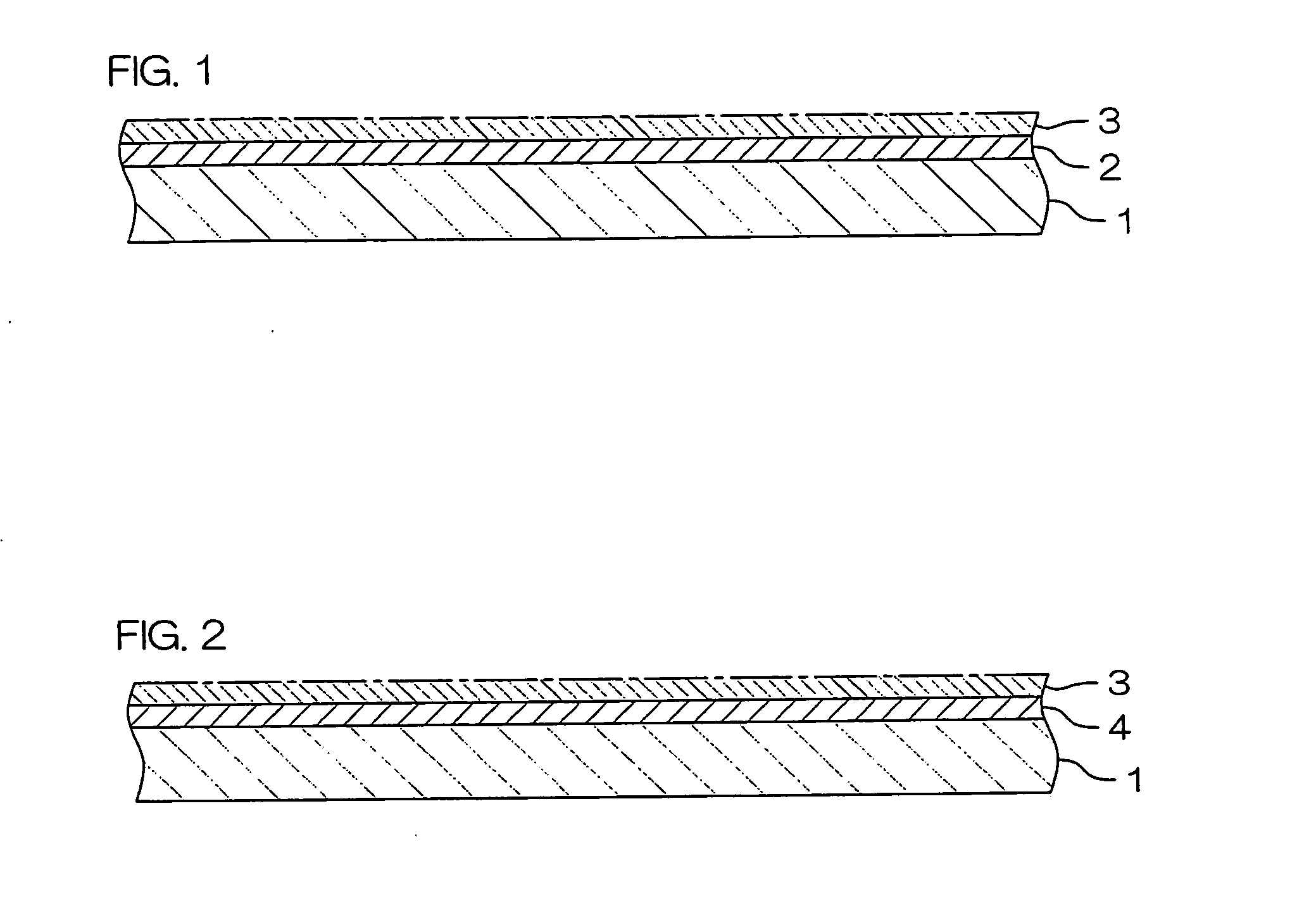
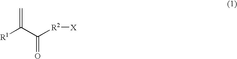
[0300] Formation of Under Coat Layer

[0301] BAYCOAT 20 (ammonium zirconium carbonate, (NH4)2[Zr(CO3)2(OH)2], ZrO2 content: 20%, manufactured by Nippon Light Metal Co., Ltd.) was diluted with a solution mixture of water and ethanol (weight ratio: 1:1) so as to adjust the ZrO2 content to 2% (Zr content: 1.48%) to prepare an undercoating solution. This undercoating solution was coated onto one side of the above-mentioned optical film using a wire bar #5, and dried at 40° C. for 2 minutes to form an under coat layer.

[0302] Production of Adhesive Film

[0303] The release film of Synthesis Example 1 was laminated on the side of the optical film, on which the under coat layer is formed, so as to contact the under coat layer with an adhesive layer, and thus an adhesive film was produced.

example 2

[0304] In the same manner as in Example 1, except that, in the formation of the under coat layer of Example 1, the ZrO2 content of 2% (Zr content: 1.48%) of the undercoating solution was replaced by the ZrO2 content of 5% (Zr content: 3.70%), an under coat layer was formed and then an adhesive film was produced.


PUM

PropertyMeasurementUnit
glass transition temperatureaaaaaaaaaa
temperatureaaaaaaaaaa
particle sizeaaaaaaaaaa

Abstract

An adhesive film prevents static charge on peeling generated when removed from an adherend and also improves adhesion between a base material and an adhesive layer, where an under coat layer containing an organometallic is formed on the base material and then an adhesive layer is formed on the base material. Alternatively, an adhesive film showing high adhesion with a glass substrate, and including an antistatic layer, which prevents static charge on peeling generated when the surface protective film is removed, and improves adhesion between a base material and an adhesive layer, where the adhesive film includes a base material, an adhesive layer made of a water dispersible adhesive including, and an antistatic layer, containing a water soluble or water dispersible conductive material, interposed between them, and the adhesive film is stuck onto an image display device.

Description

CROSS REFERENCE TO RELATED APPLICATIONS [0001] This application claims priority from Japanese Patent Application No. 2005-229927 filed Aug. 8, 2005 and Japanese Application No. 2006-091928 filed Mar. 29, 2006, the disclosures of which are herein incorporated by reference in their entirety. BACKGROUND OF THE INVENTION [0002] 1. Field of the Invention [0003] The present invention relates to an adhesive film and an image display device and, more particularly, to an adhesive film used in various industrial fields such as electrics and electronics, semiconductors and optics, and an image display device comprising the adhesive film. [0004] 2. Description of the Background Art [0005] It has hitherto been known that an adhesive film comprising a base material and an adhesive layer formed on the base material is stuck onto parts so as to protect parts in a dicing or grinding step in case of producing parts in the fields such as electrics and electronics or semiconductors. This adhesive film ...

Claims


Application Information

Patent Timeline
Patent Type & Authority Applications(United States)
IPC IPC(8): B32B7/12B32B27/30B32B37/00C09J7/29
CPCB32B7/12Y10T428/1059B32B2307/21C08K5/56C09J7/0246C09J7/0296C09J2201/128C09J2201/162C09J2205/106C09J2433/00G02F2201/50G02F2202/22G02F2202/28Y10T428/1055Y10T428/1077Y10T428/2843Y10T428/2891Y10T428/1036Y10T428/105Y10T428/2848Y10T428/2852B32B33/00C09J7/38C09J7/22C09J7/29Y10T428/31935C09J2301/162C09J2301/124C09J2301/41C09K2323/04C09K2323/035C09K2323/05C09K2323/057C09K2323/03G02F1/1333C09J133/00
Inventor KANAMARU, MIKAOKADA, KENICHITAKAHASHI, TOSHITAKA
Owner NITTO DENKO CORP
Why Eureka
Try Eureka