

Light exposure mask and method for manufacturing semiconductor device using the same
- Summary
- Abstract
- Description
- Claims
- Application Information
AI Technical Summary
Benefits of technology
Problems solved by technology
Method used
Image

Examples
embodiment mode 1
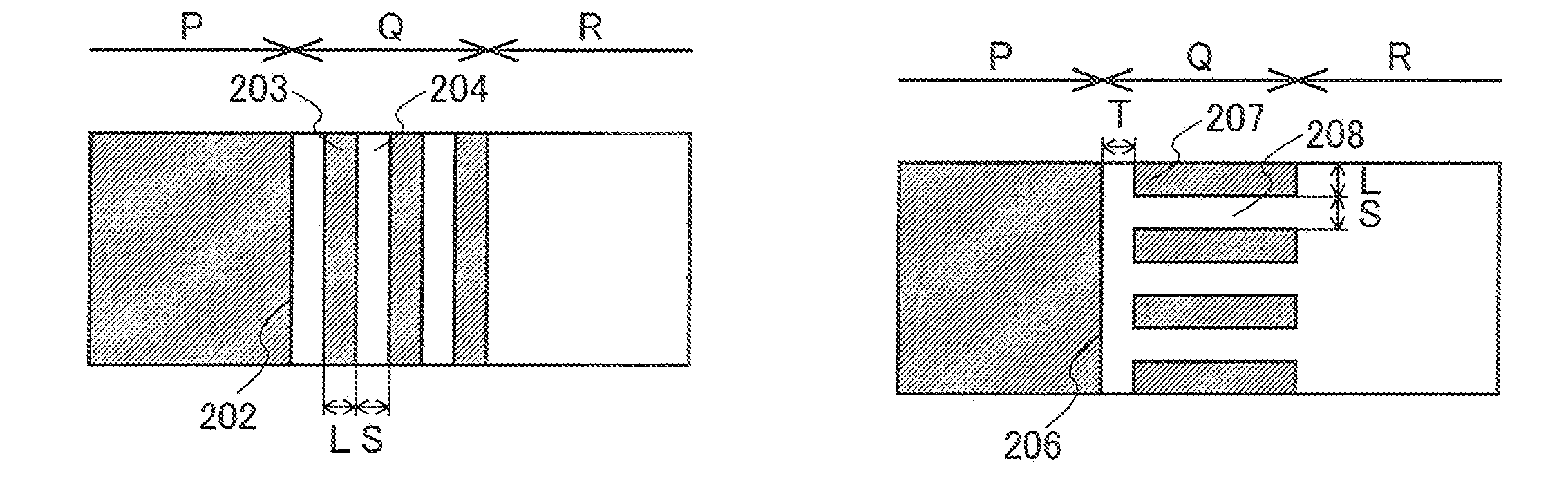
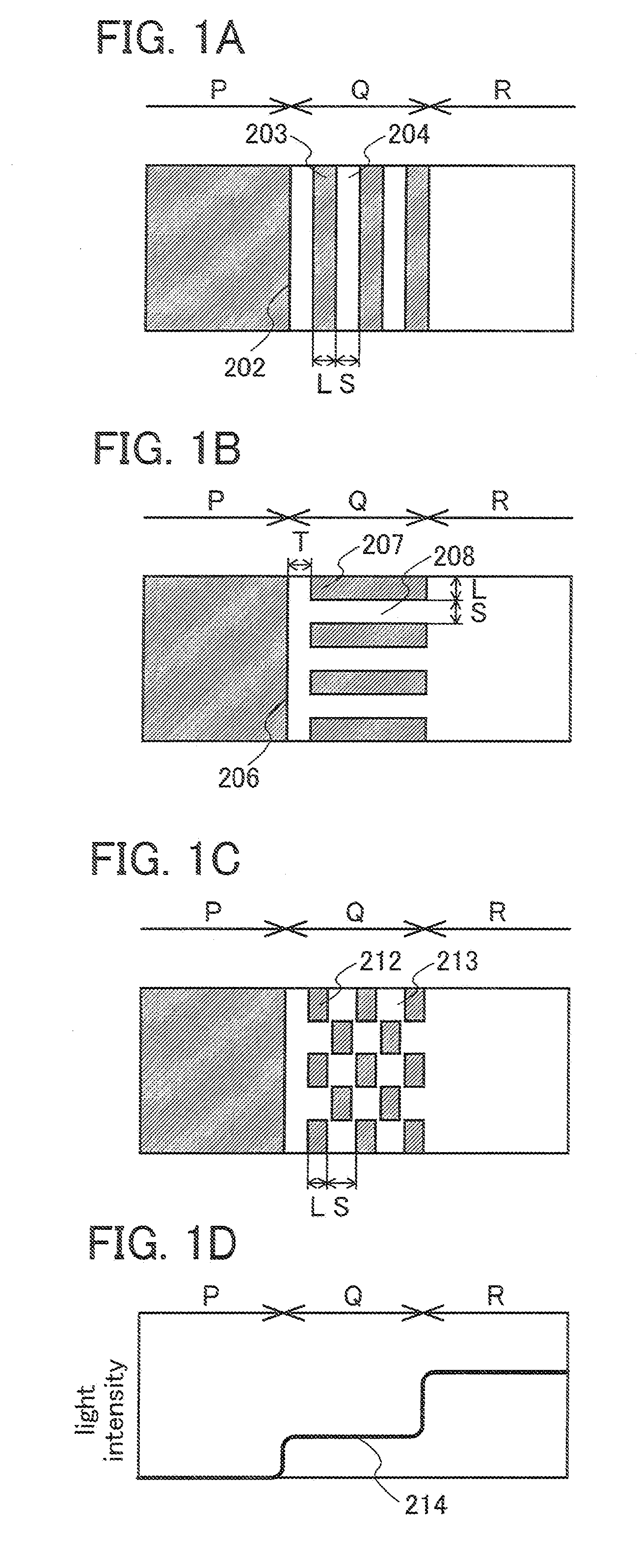
[0042] In this embodiment mode, a light exposure mask including a semi-transmissive portion formed by lines and spaces, or rectangular patterns and spaces is explained with reference to FIGS. 1A to 1D.
[0043] Specific examples of top views of light exposure masks are shown in FIGS. 1A to 1C. In addition, an example of light intensity distribution when using a light exposure mask is shown in FIG. 1D. Each of the light exposure masks shown in FIGS. 1A to 1C includes a light shielding portion P, a semi-transmissive portion Q, and a transmissive portion R. In the semi-transmissive portion Q of the light exposure mask shown in FIG. 1A, lines 203 and spaces 204 are repeatedly provided in stripes (in slits), and the lines 203 and the spaces 204 are arranged parallel to an edge 202 of the light shielding portion P. In this semi-transmissive portion, a width of each line 203 made of a light shielding material is L and a width of each space between light shielding materials is S. A light expo...
embodiment mode 2
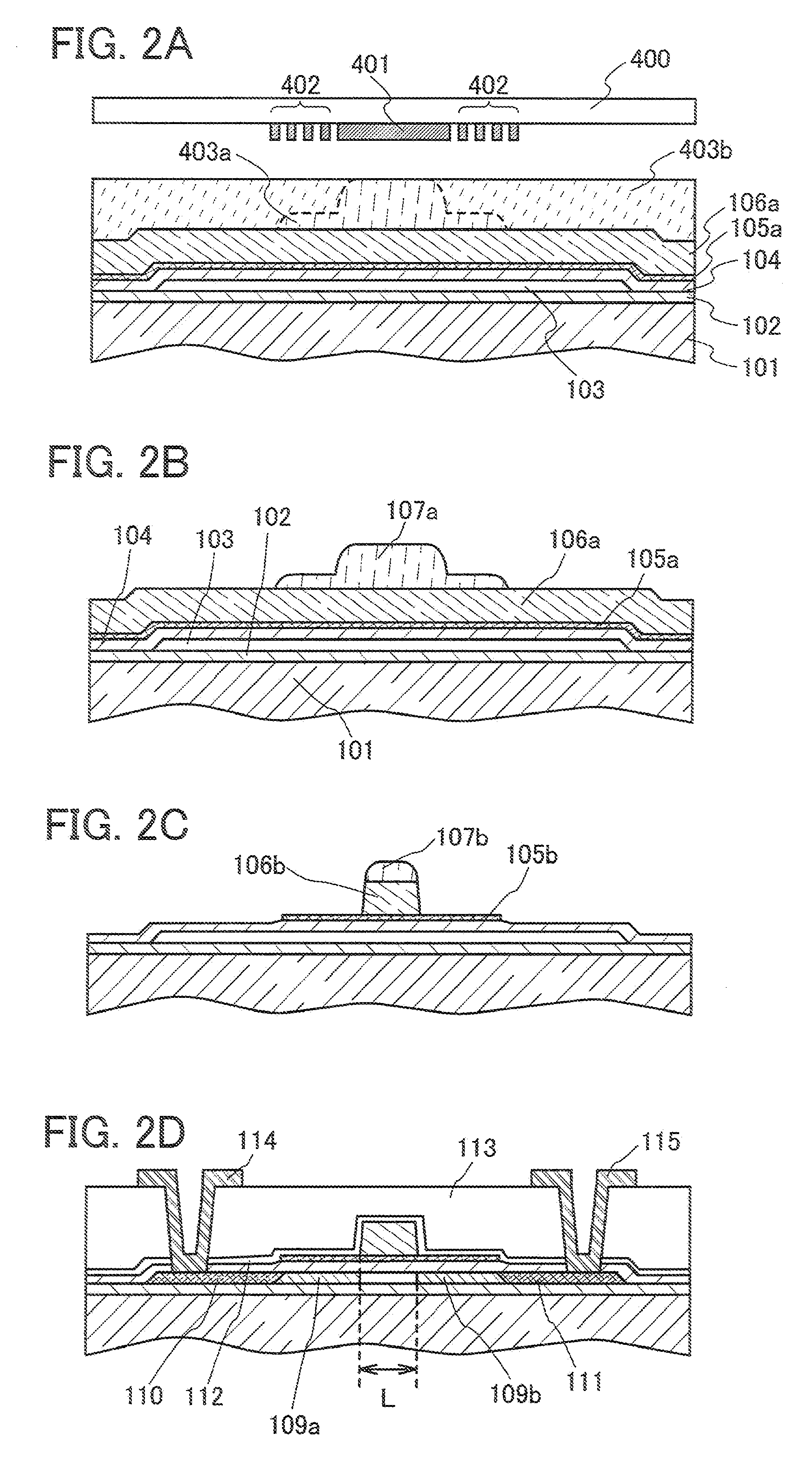
[0053] This embodiment mode describes a process of forming a gate electrode of a TFT by patterning using the light exposure mask described in Embodiment Mode 1 and forming low-concentration impurity regions on both sides of a channel formation region in a self-aligned manner by using the gate electrode as a mask at the time of ion-doping.
[0054] First, a first insulating film (base insulating film) 102 is formed over a substrate 101 having an insulating surface. As the substrate 101 having an insulating surface, a light transmitting substrate such as a glass substrate, a crystallized glass substrate, or a plastic substrate can be used. When a thin film transistor to be formed later is applied to a top-emission light emitting display device or a reflective liquid crystal display device, a ceramic substrate, a semiconductor substrate, a metal substrate, or the like can also be used.
[0055] The first insulating film 102 is formed using a single layer or stacked layers of an insulating ...
embodiment mode 3
[0110] A method for forming the conductive stacked pattern described in Embodiment Mode 2 is not particularly limited. Here, an example of forming a conductive stacked pattern by changing etching conditions a plurality of times during the process is explained with reference to FIGS. 3A to 3F.
[0111] First, similarly to Embodiment Mode 2, a resist pattern 307a is formed over a second conductive layer 306a. FIG. 3A corresponds to FIG. 2B.
[0112] Note that in FIG. 3A, a first insulating film (base insulating film) 3O2, a semiconductor layer 303, and a second insulating film (gate insulating film) 304 are formed over a substrate 301, and a first conductive layer 305a and a second conductive layer 306a are formed thereover.
[0113] Next, etching is performed under first etching conditions to form a resist pattern 307b and a second conductive layer 306b each having a step as shown in FIG. 3B. A part of the second conductive film 306b is formed into a tapered shape under the first etching c...
PUM
 Abstract
Description
Claims
Application Information