Method and apparatus for scanning and measurement by electron beam

a technology of electron beam and scanning beam, which is applied in the direction of instruments, heat measurement, nuclear engineering, etc., to achieve the effect of high precision, precise potential measurement, and reduced manufacturing cost of the apparatus

Active Publication Date: 2007-02-22
HITACHI HIGH-TECH CORP
View PDF24 Cites 45 Cited by
  • Summary
  • Abstract
  • Description
  • Claims
  • Application Information

AI Technical Summary

Benefits of technology

[0012] (2) To enhance the resolution of the SEM image, the primary electron beam is first accelerated to several keV, and then decelerated to about several hundred −1 keV by applying a retarding voltage to the wafer holder. This method is widely applied to inspecting and measurement apparatus using charged particles. Due to this, the secondary signal emitted from the surface of the semiconductor device is also accelerated by the retarding potential to several keV. However, to measure the charged potential of the wafer surface by the aforesaid energy filter, the secondary signal must be decelerated to several eV, so a strong electrostatic lens effect may occur which decreases the resolution of the primary electron beam. To avoid such an adverse effect, more grids have to be used, the energy of the secondary signal must be reduced gradually and the S curve then measured. Since the construction of the energy filter becomes more complex, the transmissivity of the secondary signal decreases and operating condition restrictions occur. (3) Due to potential distortion of the grid vicinity, the resolution of the energy filter will decrease.
[0014] The present invention therefore aims to provide a inspection and measurement apparatus and inspection and measurement method which can measure the charged potential of a sample with higher precision than the prior art technique. It also aims to provide a inspecting and measurement apparatus which can measure charged potential by means of an easy construction.
[0019] According to the invention, when measuring the surface potential of a semiconductor device, a more precise potential measurement than before, which is almost unaffected by the charged potential of the insulating film surface, can now be performed. Also, since the surface potential can be measured without an equipment specialized for wafer surface potential measurement such as an energy filter, the manufacturing cost for the apparatus can be reduced.
[0020] Further, since the surface potential of the sample can be measured with high precision, in an apparatus wherein charge control of the sample surface must be performed to control the quality of an image which is to be acquired, quality control of the acquired image is easy. This advantage is particularly useful in a inspection / measurement apparatus using a scanning electron microscope such as a critical dimension measurement SEM or SEM inspection apparatus.

Problems solved by technology

If the surface charged potential of the semiconductor device is measured by the described method, the following problem occurs:

Method used


Image

  • Method and apparatus for scanning and measurement by electron beam
  • Method and apparatus for scanning and measurement by electron beam
  • Method and apparatus for scanning and measurement by electron beam

Examples


embodiment 1

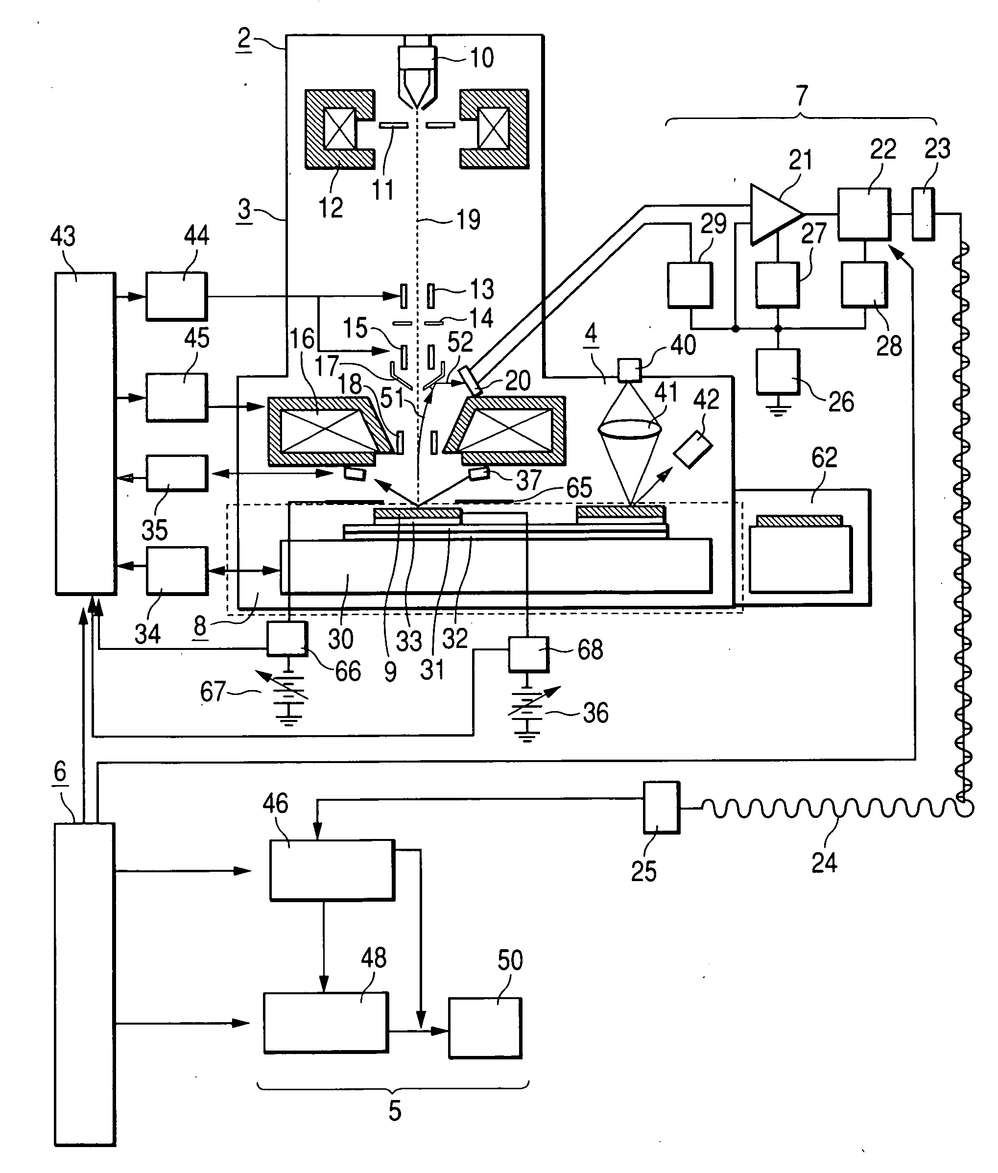
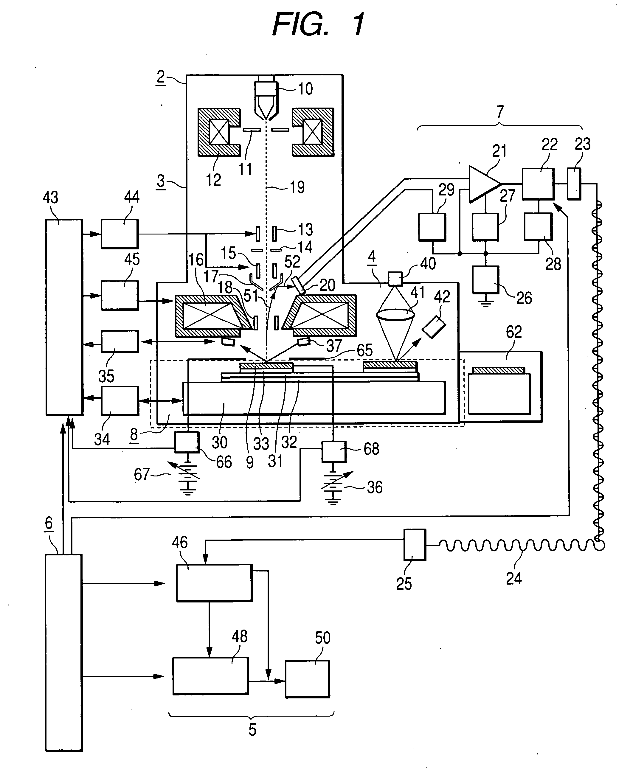
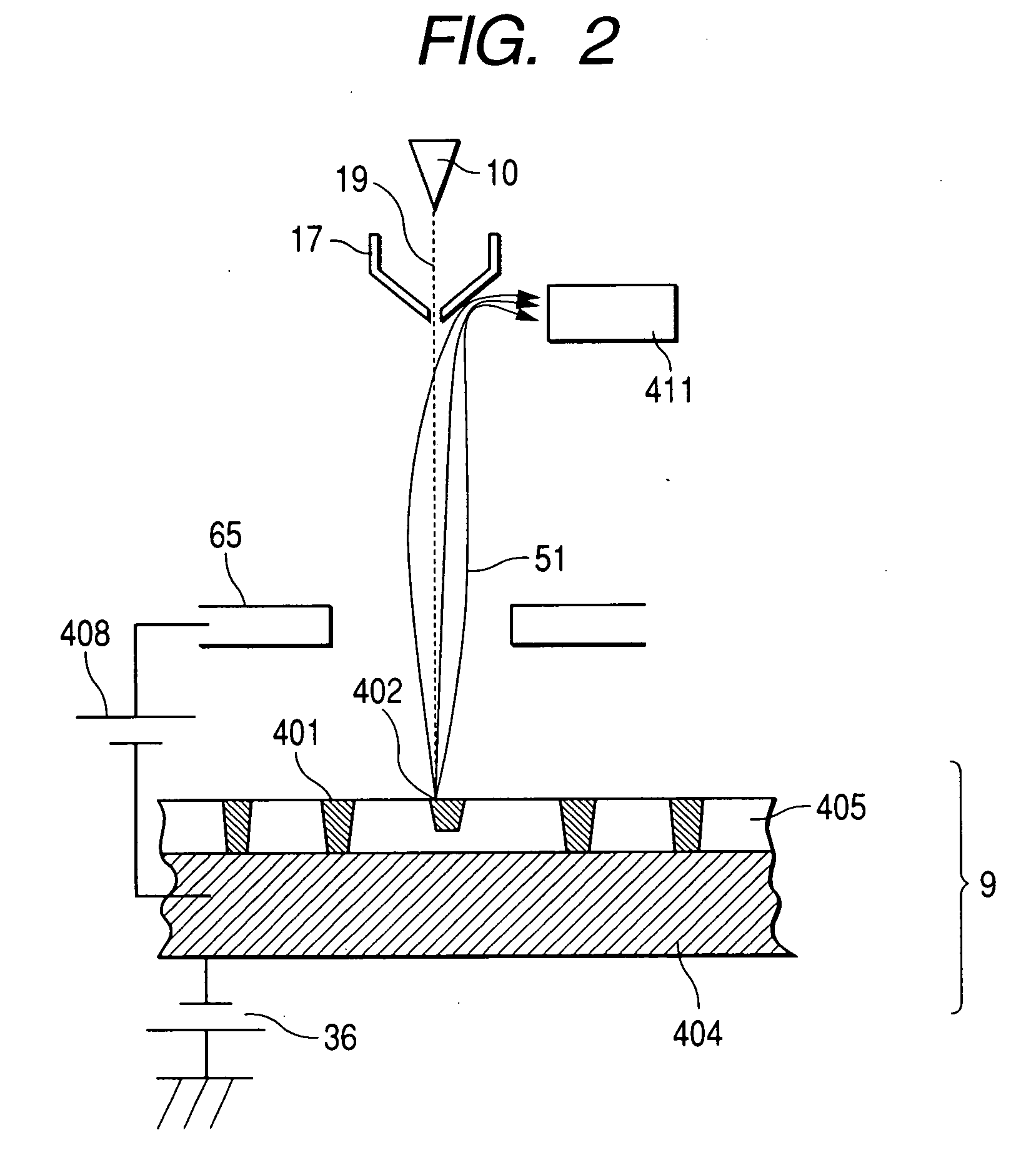
[0036]FIG. 1 shows the schematic view of the inspection apparatus relating to a first embodiment. The apparatus of this embodiment is a scanning electron microscope having a sample surface potential measurement means and charge control means, and may be applied to a inspecting SEM, review SEM and measurement SEM. The scanning electron microscope shown in FIG. 1 is provided with a chamber 2 which is placed under vacuum, and a reserve chamber (in this embodiment, not shown) for transporting a wafer 9 as sample to the interior of the chamber 2. This reserve chamber is constructed so that it can be placed under vacuum independently from the chamber 2. In addition to the chamber 2 and the reserve chamber, the apparatus comprises a controller 6 and image processor 5. The interior of the chamber 2 broadly comprises an electron optics system 3, charge controller, detector 7, sample chamber 8 and optical microscope 4. In this embodiment, the chamber 2 means the whole vacuum vessel containing...

embodiment 2

[0071] If there are plural types of patterns in the wafer, the charged potential of each pattern will be different even if a precharge is performed on the whole wafer prior to the inspection. In this embodiment, a method will be described for determining the inspection conditions in this case.

[0072] In a die 252 of a wafer 251 of FIG. 8, patterns 255, 256 were made, respectively. From measurements by the method of the flow chart 200 for charged potential measurement of a specific region, the electrostatic potentials of the regions 253, 254 were −5V and −10V, respectively. In this case, (1) the average value of the optimum inspection conditions (e.g., Vcc value) estimated for both regions was used, or (2) the measurement was performed plural times varying the inspection conditions for each pattern, these methods being selected as required. Method (1) has an advantage that the inspection time is short as the whole surface is inspected under the same conditions, even though the inspec...

embodiment 3

[0073] In this embodiment, an example will be described where a pattern dimensional measurement was performed using a length measuring SEM.

[0074]FIG. 9 shows an example of the construction of the length measurement SEM of this embodiment. The apparatus comprises an electron optical system 301, stage mechanism system 315, wafer transport system 322, vacuum discharge system 305, optical microscope 325, control system 331, control unit 332, and electrostatic controller.

[0075] The electron optical system 301 comprises an electron source 302, condenser lens 303, objective lens 312, first detector 310, second detector 307, deflector 308, reflecting plate 309, and wafer height detector 313. Reflected electrons 311 and secondary electrons 306 emitted by irradiating a wafer 316 with a primary electron beam 304 are detected by the first detector 310 and second detector 307, respectively.

[0076] The stage mechanism system 315 comprises an XY stage 318, holder 317 for mounting a wafer as a sa...


PUM

PropertyMeasurementUnit
resistanceaaaaaaaaaa
electrostatic potentialsaaaaaaaaaa

Abstract

A inspecting and measurement method and inspecting and measurement apparatus for semiconductor devices and patterns such as photomasks using an electron beam which can measure the charged potential of a sample with higher precision than in the prior art, and a inspecting and measurement apparatus which can measure charged potential by means of a simple construction. When an S curve is observed in a semiconductor device to be inspectioned and measured, fluctuations of the charged potential of the inspection sample surface are suppressed by optimizing the energy of a primary electron beam used for irradiation. When the surface potential of the semiconductor device is measured, a more precise potential measurement than that of the prior art can be performed which is almost unaffected by the charged potential of an insulation film surface. Further, the surface potential can be measured without installing a special apparatus for wafer surface potential measurement such as an energy filter, so the cost of the apparatus can be reduced.

Description

CLAIM OF PRIORITY [0001] The present application claims priority from Japanese application JP No. 2005-238105 filed on Aug. 19, 2005, the content of which is hereby incorporated by reference into this application. FIELD OF THE INVENTION [0002] The present invention relates to a method of manufacturing a fine circuit pattern formed on a substrate such as a semiconductor device or liquid crystal, and in particular relates to a method of pattern inspecting and measurement of a semiconductor device and photomask by an electron beam. BACKGROUND OF THE INVENTION [0003] A semiconductor device is manufactured by repeatedly performing a process which transfers a pattern formed on a photomask to a semiconductor wafer by lithography and etching. In this manufacturing process, the quality of lithography, etching and other steps, and the production of foreign matter, largely affect the yield of the semiconductor device, so in the semiconductor manufacturing field, it is important to have a metho...

Claims


Application Information

Patent Timeline
Patent Type & Authority Applications(United States)
IPC IPC(8): G21K7/00G01N23/00
CPCG01N23/2251G01R31/307H01J37/026H01J37/28H01J2237/2817H01J2237/0047H01J2237/0048H01J2237/2816H01J2237/0044
Inventor CHENG, ZHAOHUIMAKINO, HIROSHIKOYAMA, HIKARUSATO, MITSUGU
Owner HITACHI HIGH-TECH CORP
Why Eureka
Try Eureka