Electrostatic discharge protection element

Active Publication Date: 2007-02-22
INFINEON TECH AG
View PDF21 Cites 76 Cited by
  • Summary
  • Abstract
  • Description
  • Claims
  • Application Information

AI Technical Summary

Benefits of technology

[0075] In a device for protection against electrostatic discharges in accordance with another embodiment of the invention, a ballast resistor is connected in series in each fin of a transistor to be protected (e.g. driver transistor). During a normal operating state, the ballast resistors connected in series are at low resistance and therefore have only an insignificant influence on the current flow through the individual fins. During an ESD event, the ballast resistors acquire high resistance and a homogeneous current distribution between all the

Problems solved by technology

The development of efficient protection mechanisms for protecting an electronic component against ESD constitutes a growing challenge, particularly when using advanced process technologies such as, for example, MuGFET technologies or FinFET technologies, in view of the ever shrinking dimensions of the electronic devices and the associated increasing sensitivity toward electrical overvoltages.
Electrostatic discharges (ESD) represent a permanent threat to integrated circuits (IC).
During an ESD event, short electrical discharge pulses occur during which high electric currents flow or high electrical voltages occur which can damage one or more electronic components of the circuit.
The fin structure results for example in a poor thermal conduction of the devices, which leads to an extremely high intrinsic susceptibility.
To express it clearly, during an ESD discharge during which a high current flows through the fin, the poor heat dissipation means that severe heating of the fin structure can occur, which may lead to burn-out of the fin.
The development of effective ESD protection elements in FinFET technologies or MuGFET technologies constitutes a major technological challenge.
One problem consists in achieving a uniform distribution of the electric current over the entire width of the transistor in order thereby to minimize the

Method used


Image

  • Electrostatic discharge protection element
  • Electrostatic discharge protection element
  • Electrostatic discharge protection element

Examples


Embodiment Construction

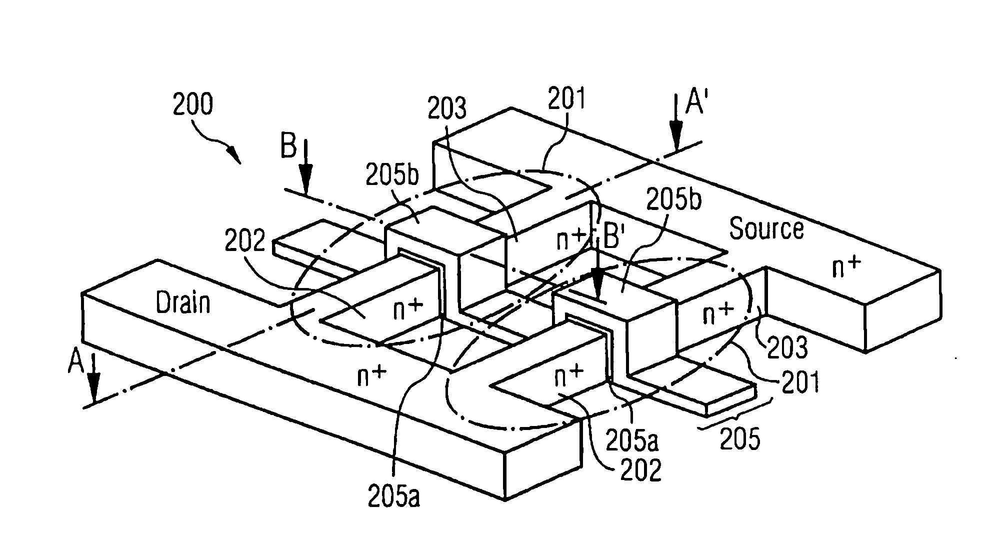
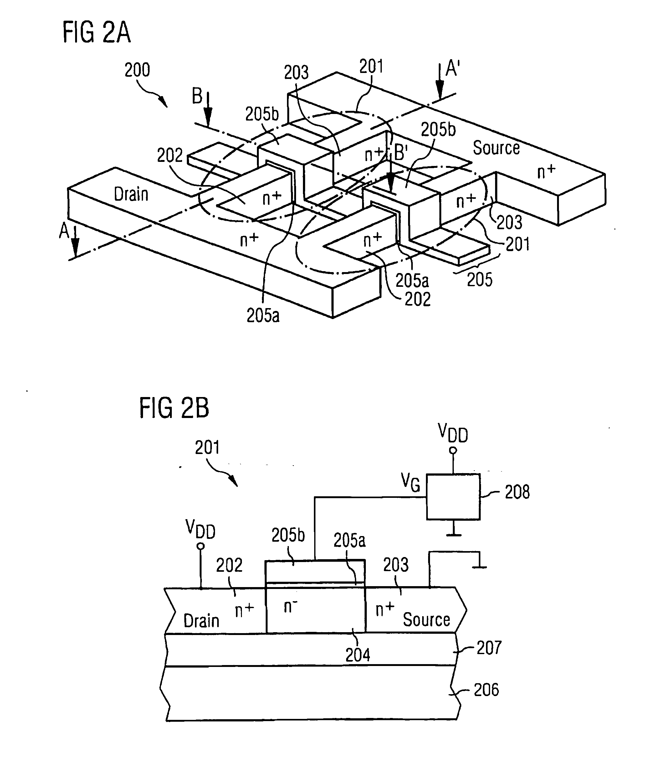
[0099]FIG. 2A shows a device 200 for protection against electrostatic discharges in an electrical circuit with two gate controlled fin resistance elements 201 formed as fin junction field effect transistors (FinJFET) in accordance with one exemplary embodiment of the invention. The gate controlled fin resistance elements 201 have a fin structure, having in each case a heavily n doped (n+ doped) first connection region 202, a heavily n doped (n+ doped) second connection region 203 and also a weakly n doped (n− doped) channel region 204 formed between the first connection region 202 and the second connection region 203, the channel region 204 being concealed by a gate region or gate 205 formed over the side areas and the upper face of the channel region 204, cf. FIG. 2B.

[0100] The fin structures of the gate controlled fin resistance elements 201 have for example a length of between 10 nm and 10 μm, and a width of between 5 nm and 50 nm, and a height of between 5 nm and 200 nm.

[0101]...


PUM


Abstract

A gate controlled fin resistance element for use as an electrostatic discharge (ESD) protection element in an electrical circuit has a fin structure having a first connection region, a second connection region and a channel region formed between the first and second connection regions. Furthermore, the fin resistance element has a gate region formed at least over a part of the surface of the channel region. The gate region is electrically coupled to a gate control device, which gate control device controls an electrical potential applied to the gate region in such a way that the gate controlled fin resistance element has a high electrical resistance during a first operating state of the electrical circuit and a lower electrical resistance during a second operating state, which is characterized by the occurrence of an ESD event.

Description

CROSS-REFERENCE TO RELATED APPLICATION [0001] This application is claims priority to German Patent Application No. DE 10 2005 039 365.9-33 filed Aug. 19, 2005. BACKGROUND [0002] 1. Technical Field [0003] The invention relates to a gate controlled fin resistance element for use as electrostatic discharges (ESD) protection element in an electrical circuit, and to a device for protection against electrostatic discharges in an electrical circuit. [0004] 2. Description of the Related Art [0005] The development of efficient protection mechanisms for protecting an electronic component against ESD constitutes a growing challenge, particularly when using advanced process technologies such as, for example, MuGFET technologies or FinFET technologies, in view of the ever shrinking dimensions of the electronic devices and the associated increasing sensitivity toward electrical overvoltages. [0006] Electrostatic discharges (ESD) represent a permanent threat to integrated circuits (IC). During an ...

Claims


Application Information

Patent Timeline
IPC IPC(8): H01L23/62
CPCH01L27/0288H01L27/1211H01L29/66795H01L29/785H01L29/8086H01L2029/7857H01L29/42392
Inventor GOSSNER, HARALDRUSS, CHRISTIAN
Owner INFINEON TECH AG
Why Eureka
Try Eureka