Nonvolatile memory cell, storage device and nonvolatile logic circuit

Inactive Publication Date: 2007-02-22
SONY SEMICON SOLUTIONS CORP
View PDF7 Cites 67 Cited by
  • Summary
  • Abstract
  • Description
  • Claims
  • Application Information

AI Technical Summary

Benefits of technology

[0008] However, the write/erase speed of the flash memory for backing up the data is slow, i.e., 10 microseconds to 10 millisec

Problems solved by technology

However, the write/erase speed of the flash memory for backing up the data is slow, i.e., 10 microseconds to 10 milliseconds.
This is inconvenient in the operation of a system frequently turning on/off the power for reducing the power consumption.
However, when the power is turned off, the information is erased, therefore the required data is stored in a separately provided nonvolatile memory befo

Method used


Image

  • Nonvolatile memory cell, storage device and nonvolatile logic circuit
  • Nonvolatile memory cell, storage device and nonvolatile logic circuit
  • Nonvolatile memory cell, storage device and nonvolatile logic circuit

Examples


Example

First Embodiment

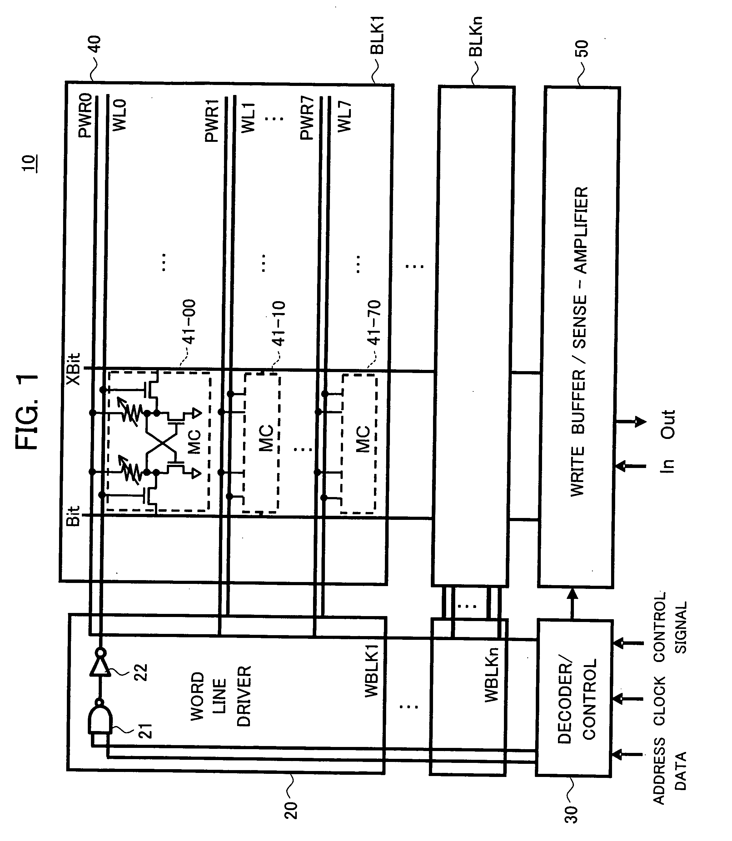
[0054]FIG. 1 is a block diagram of the configuration of a nonvolatile storage device 10 according to an embodiment of the present invention.

[0055] The nonvolatile storage device 10 is configured by a word line driver (word driver) circuit 20, a decoder / control circuit 30, a write buffer / sense-amplifier (Sense-Amp) circuit 50, a memory cell MC portion 40, etc.

[0056] In FIG. 1, for simplification, only one word driver circuit 20 and one memory block BLK1 are shown, but there are actually 2n / 23 memory blocks (BLK1) in which word lines are arranged in units of for example 23 (n is a positive integer and number of row address bits).

[0057] In FIG. 1, there are 23 word lines in the blocks (WBLK1 to WBLKn) of the word driver circuit 20. These are shown as WL0 to WL7. Memory cells MC (41-00, 41-10, . . . , 41-70, . . . ) are connected to the word lines (lines).

[0058] The decoder / control circuit 30 is configured by a pre-decoder, an internal timing control circuit, etc. a...

Example

Second Embodiment

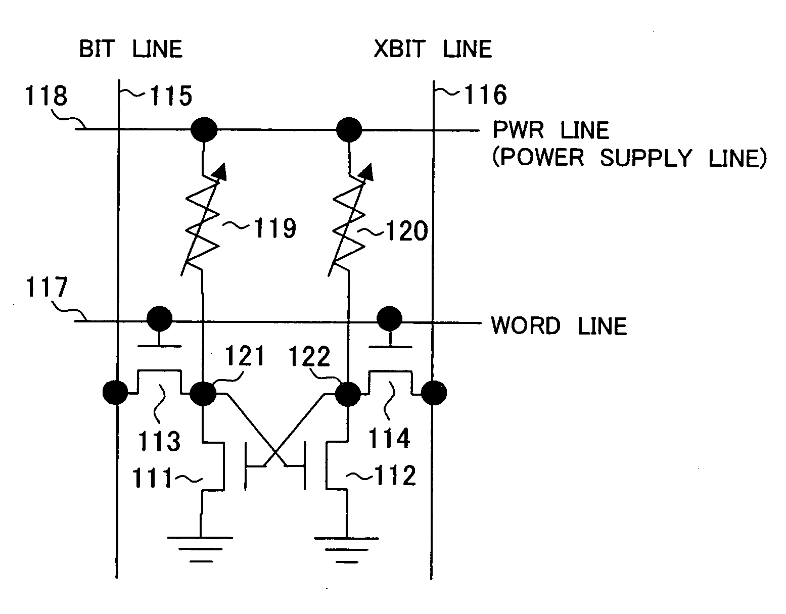
[0081] In a memory cell MC100 shown in FIG. 2, a drain of an N channel metal oxide semiconductor (NMOS) transistor 111 is connected to a drain / source of an NMOS transistor 113 of the transfer gate and one terminal of a variable resistance element 119, a gate of the transistor 111 is connected to the drain of an NMOS transistor 112, and a source of the transistor 111 is connected to a reference voltage for example GND (ground).

[0082] The other terminal of the variable resistance element 119 is connected to a power supply (PWR) line 118. The gate of the NMOS transistor 113 is connected to a word line 117, and its source / drain is connected to a bit line 115.

[0083] In the same way, the drain of the NMOS transistor 112 is connected to the drain / source of an NMOS transistor 114 of the transfer gate and one terminal of a variable resistance element 120, its gate is connected to the drain of the NMOS transistor 111, and its source is connected to the reference voltage fo...

Example

Third Embodiment

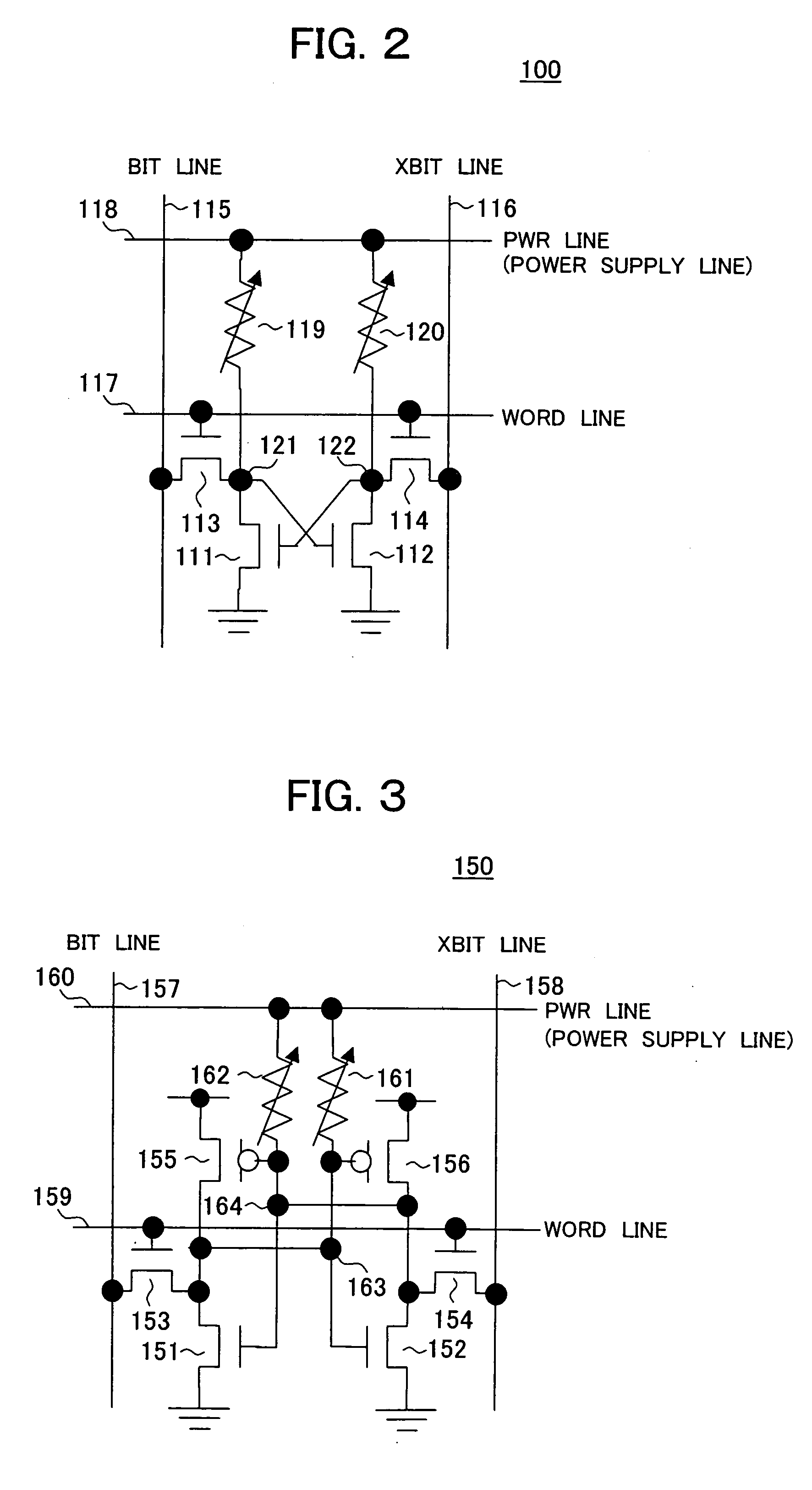
[0086]FIG. 3 shows the circuit configuration of a memory cell MC150 as another embodiment.

[0087] The memory cell MC150 shown in FIG. 3 is configured by PMOS transistors 155 and 156, NMOS transistors 151, 152, 153, and 154, and variable resistance elements 161 and 162.

[0088] A word line 159 is connected to gates of the NMOS transistors 153 and 154 of the transfer gate, and a bit line 157 and an inverted bit (XBit) line 158 are connected to drains / sources of the NMOS transistors 153 and 154.

[0089] The source of the PMOS transistor 155 is connected to the power supply, and its drain is connected to the drain of the NMOS transistor 151 and the source / drain of the NMOS transistor 153. Further, the source of the NMOS transistor 151 is connected to a reference potential, for example, the GND (ground).

[0090] In the same way, the source of the PMOS transistor 156 is connected to the power supply, and its drain is connected to the drain of the NMOS transistor 152 and the ...


PUM


Abstract

One or serially connected field effect transistors are cross coupled with each other, first terminals of nonvolatile variable resistance elements are connected to their storage nodes, and the other terminals of the variable resistance elements are connected to a power supply line to thereby form a memory cell. By controlling the voltage supplied to this power supply line, data of the memory cell immediately before turning off the power is stored in it when the power is turned off.

Description

CROSS REFERENCE TO RELATED APPLICATION [0001] The present invention contains subject matter related to Japanese Patent Application No. 2005-238609 filed in the Japan Patent Office on Aug. 19, 2005 and Japanese Patent Application No. 2005-245997 filed in the Japan Patent Office on Aug. 26, 2005, the entire contents of which being incorporated herein by reference. BACKGROUND OF THE INVENTION [0002] 1. Field of the Invention [0003] The present invention relates to a nonvolatile memory cell obtained by using a resistance element including two electrode films between which a recording film is sandwiched and given voltages having different polarities at its two electrodes to reversibly change the resistance value of the recording film, that is, a so-called nonvolatile variable resistance type storage element, to replace a p-channel metal oxide semiconductor (PMOS) transistor of a six-transistor-type static random access memory (SRAM) memory cell or adding this to a six-transistor-type SRA...

Claims


Application Information

Patent Timeline
IPC IPC(8): G11C11/00
CPCG11C11/412G11C13/0002G11C13/0061G11C13/0069G11C14/009G11C2013/0073G11C16/06G11C16/30
Inventor OKAZAKI, NOBUMICHISHIIMOTO, TSUNENORIHACHINO, HIDENARIOTSUKA, WATARU
Owner SONY SEMICON SOLUTIONS CORP
Why Eureka
Try Eureka