However, a via having a spot area diameter of less than 50 μm cannot be formed using a CO2 laser.
The high degree of
reflectivity of
copper at the CO2
wavelength makes very difficult the formation of a through-hole via using a CO2 laser in a
copper sheet having a thickness greater than about 5 microns.
Thus, laser processing
throughput, such as, for example, via formation on PCB or other
electronic packaging devices or hole drilling on metals or other materials, is limited by the laser power available and pulse repetition rate, as well as the speed at which the beam positioner can move the laser output in a spiral, concentric circle, or trepan pattern and between via positions.
However, for the UV DPSS laser and the pulsed CO2 laser, as pulse repetition rates increase, pulse power decreases in a non-linear fashion, i.e., twice the pulse repetition rate results in less than one-half the pulse power for each pulse.
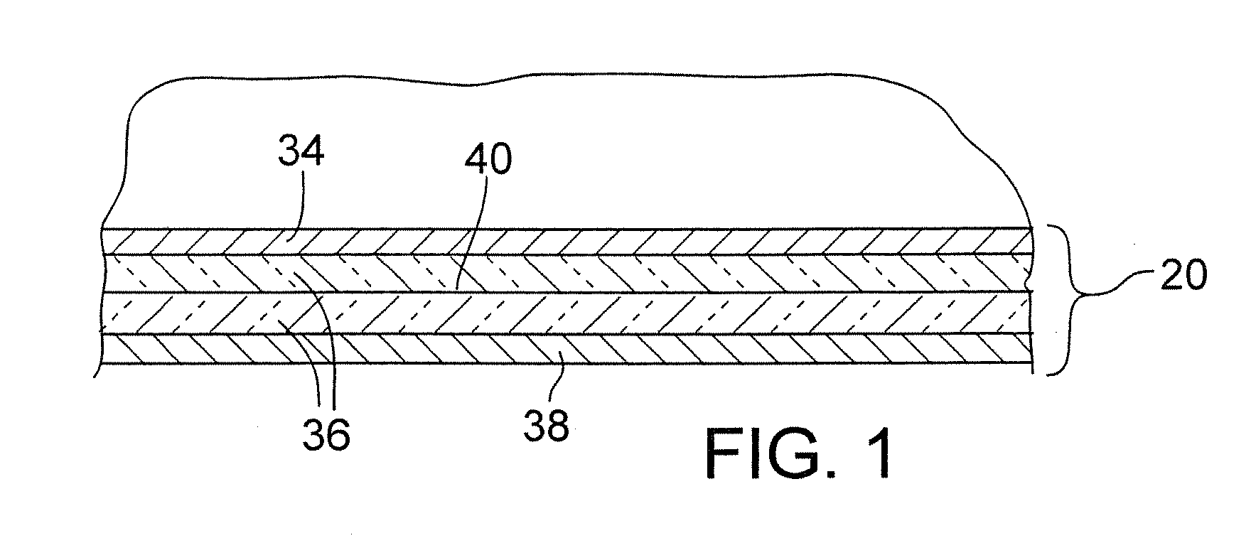
Mechanically sawing wafers having a thickness that is less than about 100 microns results in
cracking of the
wafer.
However, one
disadvantage of laser dicing
semiconductor wafers is the formation of debris and
slag, both of which could adhere to the wafer and are difficult to remove.
Another
disadvantage of laser dicing semiconductor wafers is that the workpiece
throughput rate is limited by the power capabilities of the laser.
One problem with
laser micromachining operations as discussed herein is that, due to non-uniformities in the workpiece, performing the
machining operations with the same laser parameters at two different locations on the workpiece can result in differences in feature qualities.
Furthermore these variations can be repetitive from workpiece to workpiece in a given lot of workpieces due to normal variations in manufacturing tolerances.
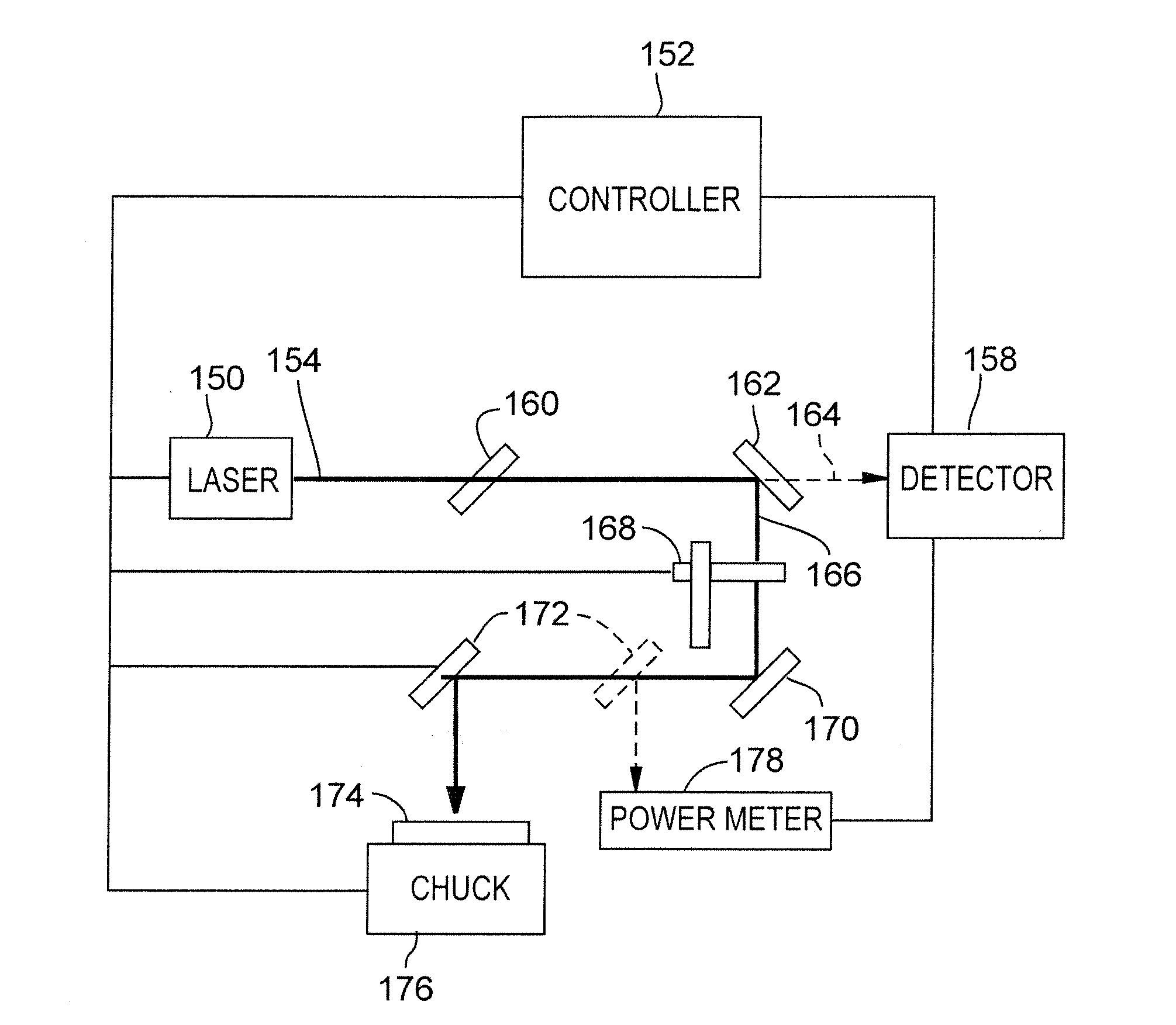
As optical components age, they are subject to
contamination, most notably from debris from the micromachining operation itself and damage from the high-power
laser beams being transmitted through the
optics.
These and other forms of degradation can cause the laser spot projected onto the workpiece to change in size, shape, intensity or other characteristics, thereby changing the size, shape, depth, or other measures of the feature being micromachined in
spite of the exact same parameters being used to control the laser beam.
The problem with this approach is that although it can help compensate for aging
optics or other sources of variation in laser power, the fact that it is automatically compensating for possible deterioration of the laser or optics means that, unless the system is monitored, there is concealment of important information that could be used to trigger maintenance of the system before the system shuts down and valuable production time is lost.
Another issue with trying to maintain consistent quality of laser micromachined feature is that simply recording pre-selected laser parameters such as
pulse repetition frequency (PRF) or
pulse energy, among others, is not sufficient to characterize the laser parameters used in the micromachining process because the laser beam is typically not directed at the workpiece for the total nominal duration of the micromachining process.
If the nominal laser energy value cannot be reached by adjusting the attenuator, the system generates an
error signal.
The problem is that unless the system is able to
record the attenuator setting, the final laser power, and the number of pulses actually delivered to the workpiece, among other parameters, over the specific period of time the feature is being micromachined as opposed to being calibrated, there will exist no accurate
record of the actual laser power directed at the workpiece during the micromachining of a particular feature.
The complexity of the toolpath is such that it is subject to repeatable transient behavior that affect the efficiency with which the laser beam interacts with the workpiece.
These delays affect the internal state of the laser, due to variations in
stored energy in the lasing medium and thermal transients of
optical cavity components.

