Method of solder bumping a circuit component and circuit component formed thereby

a technology of circuit components and solder bumps, which is applied in the direction of semiconductor devices, semiconductor/solid-state device details, electrical apparatus, etc., can solve the problems of “electrically open” solder joints, general unsolderability and corrosion of aluminum and its alloys, and reduce the efficiency of solder bumping, so as to prevent or at least reduce the effect of solder connection degradation by electromigration

Inactive Publication Date: 2007-03-01
DELPHI TECH INC
View PDF18 Cites 81 Cited by
  • Summary
  • Abstract
  • Description
  • Claims
  • Application Information

AI Technical Summary

Benefits of technology

[0007] The present invention provides a circuit component and method by which degradation of a solder connection by electromigration can be prevented or at least reduced.
[0010] In view of the above, it can be seen that the stud within the solder material defines part of the conductive path through the solder material. By forming the stud of a highly conductive material, such as copper, the stud can provide a low electrical resistance path through the solder material to advantageously decrease the current density through an electrical connection subsequently formed by the solder material. If the stud is formed of copper and the solder material contains tin, such as a SnPb solder, the stud can also serve as a source of copper to form a desirable SnCu intermetallic layer capable of reducing or eliminating dissolution of the multilayer structure.
[0012] Other advantages of the present invention include the relatively low cost of incorporating a wire bonding step into a solder bumping operation that can otherwise be entirely conventional aside from the wire-bonding operation, and the minimally negative and potentially beneficial affect that studs formed of appropriate material have on the thermal resistance of the solder connections containing the studs. As a result, incorporation of studs does not negatively affect the thermal management of the device, and if formed of a highly thermally conductive material such as copper, can increase the thermal conductivity of a solder connection. Accordingly, the stud can promote heat flow through the connection and reduce the temperature of the connection, further reducing the tendency for electromigration to occur.

Problems solved by technology

Aluminum and its alloys are generally unsolderable and susceptible to corrosion if left exposed, and copper is readily dissolved by molten solder.
This segregation is detrimental to the long term reliability and performance of the solder bump connection, and in some cases can lead to “electrically open” solder joints.
Electromigration is typically the limiting factor for determining the maximum current capability for a flip chip IC.
However, the relatively thick plated copper pillar causes high mechanical stress on the surface of the silicon IC and it's interconnect and passivation structures, which can lead to fracture of those structures due to mechanical and / or environmental stresses.

Method used


Image

  • Method of solder bumping a circuit component and circuit component formed thereby
  • Method of solder bumping a circuit component and circuit component formed thereby
  • Method of solder bumping a circuit component and circuit component formed thereby

Examples


Embodiment Construction

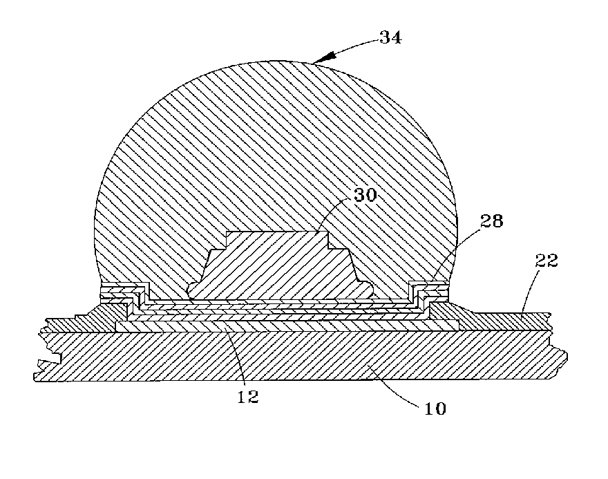
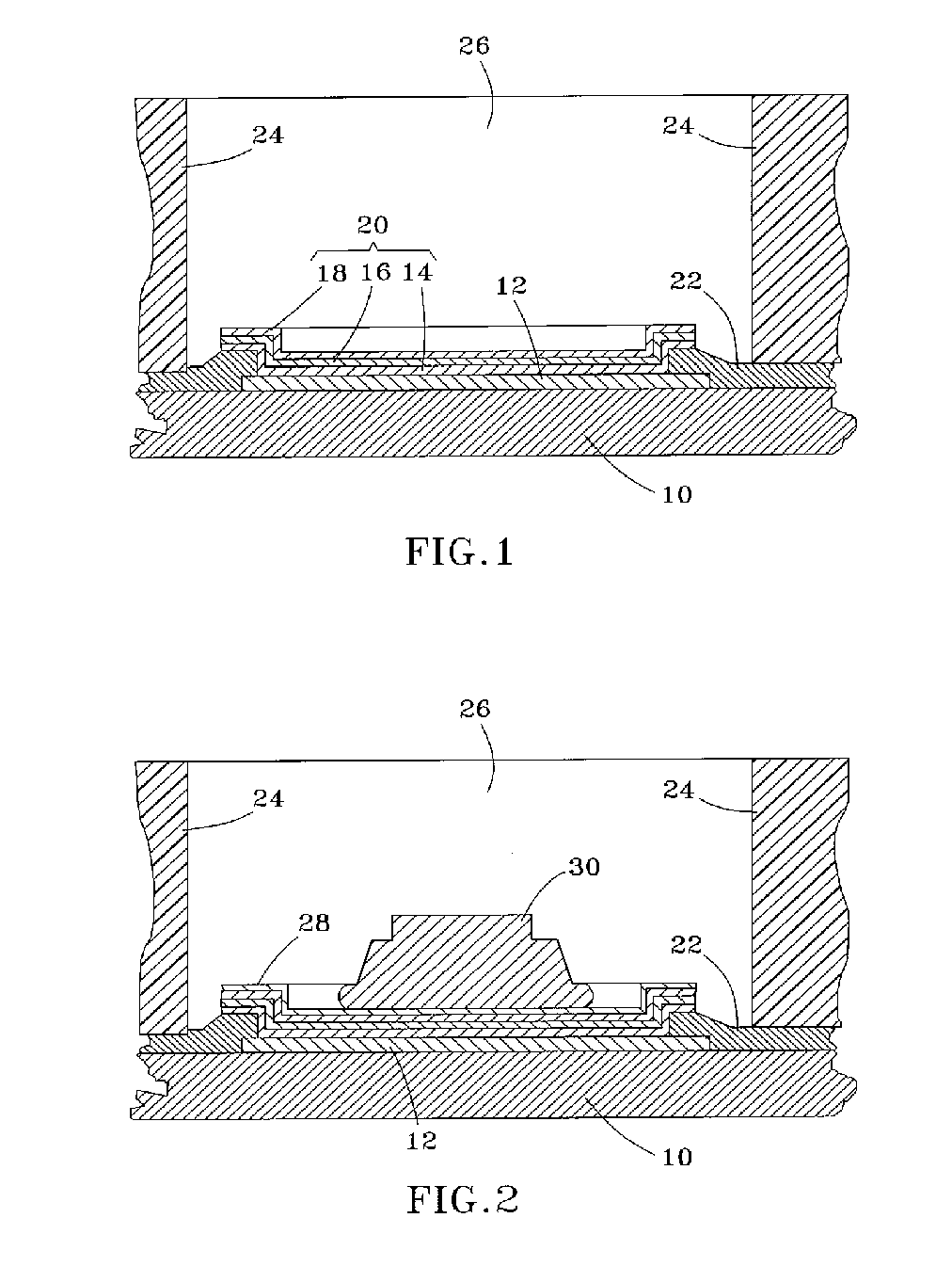
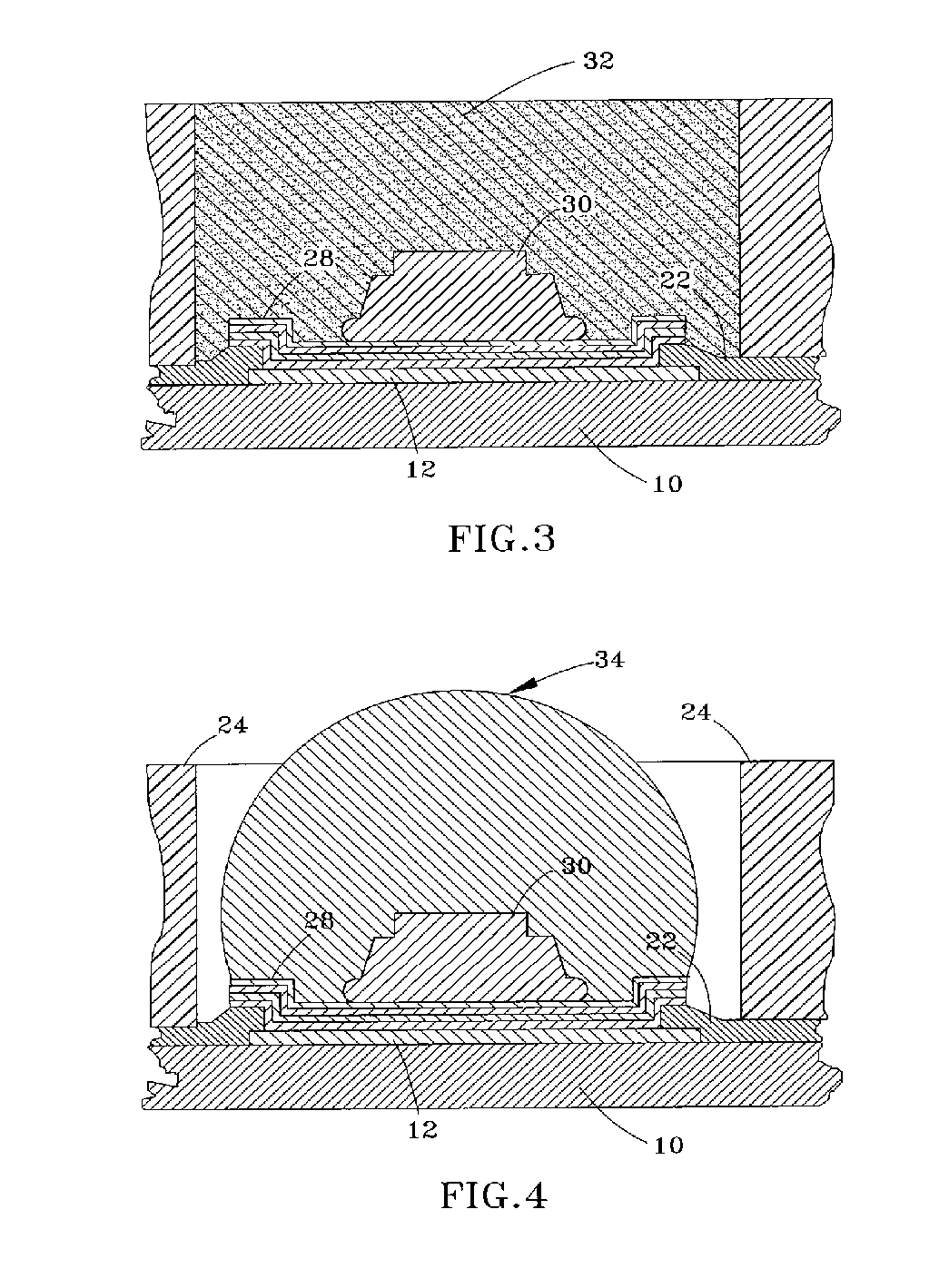
[0016]FIGS. 1 through 5 represent partial cross-sectional views of a surface region of a semiconductor die 10, such as a flip chip, as it is prepared for and then undergoes solder bumping in accordance with the present invention. As described previously, FIG. 1 shows the surface of the die 10 as being protected by a passivation layer 22 that, as known in the art, protects the die 10 from environmental contaminants, moisture, and electrical shorts. The passivation layer 22 is typically silicon dioxide, though silicon nitride, polyimides, phosphosilicated glass (PSG), borophosphosilicated glass (BPSG), or organic layers such as polyimide, BCB (benzocyclobutene), or PBO (polybutylene oxide) may also be used. A portion of a runner is exposed by an opening in the passivation layer 22, defining what is termed herein an interconnect pad 12. The runner and pad 12 can be conventionally formed of aluminum or an aluminum-base alloy, which renders the pad 12 generally unsolderable and susceptib...


PUM

PropertyMeasurementUnit
thicknessesaaaaaaaaaa
thicknessaaaaaaaaaa
temperatureaaaaaaaaaa

Abstract

A circuit component and method by which degradation of a solder connection by electromigration can be prevented or reduced. The component generally includes an interconnect pad on a surface of the component, a metallic multilayer structure overlying the interconnect pad and having a solderable surface layer, and a solder material on the multilayer structure. According to a preferred aspect of the component and method, a stud is wire-bonded to the solderable surface layer of the multilayer structure and encased by the solder material to provide a low electrical resistance path through the solder material.

Description

BACKGROUND OF THE INVENTION [0001] The present invention generally relates to integrated circuit (IC) devices attached by solder bumps. More particularly, this invention relates to a method of solder bumping a circuit component to yield a solder connection that is resistant to electromigration. [0002] A flip chip is attached to circuit board or other suitable substrate with beadlike terminals formed on interconnect pads located on one surface of the chip. The terminals are typically in the form of solder bumps near the edges of the chip, which are reflowed to both secure the chip to the circuit board and electrically interconnect the flip chip circuitry to a conductor pattern on the circuit board. Reflow soldering techniques generally require that a controlled quantity of solder or solder paste is deposited on the chip pads using methods such as electrodeposition and printing. The solder or solder paste is then heated above the melting or liquidus temperature of the solder alloy (fo...

Claims


Application Information

Patent Timeline
Patent Type & Authority Applications(United States)
IPC IPC(8): H01L23/48H01L21/44
CPCH01L24/11H01L2924/014H01L2224/1147H01L2224/13099H01L2924/01013H01L2924/01022H01L2924/01029H01L2924/01046H01L2924/01047H01L2924/01074H01L2924/01078H01L2924/01079H01L2924/01082H01L2924/01322H01L2924/01327H01L2924/14H01L2924/01006H01L2924/01023H01L2924/01024H01L2924/01033H01L24/12H01L2224/05027H01L2224/05022H01L2224/0508H01L2224/05001H01L2224/05572H01L2224/05124H01L2224/05144H01L2224/05147H01L2224/056H01L2224/05644H01L2224/05647H01L2224/05664H01L2224/05164H01L2224/05166H01L2224/05171H01L2224/05184H01L2224/1134H01L2224/11312H01L2224/11849H01L2224/13076H01L2224/131H01L2224/13147H01L2224/13144H01L2224/13139H01L2224/13164H01L2224/13169H01L24/13H01L24/05H01L2924/00014
Inventor VARNAU, MICHAEL J.
Owner DELPHI TECH INC
Why Eureka
Try Eureka