Flat-panel display

a technology of flat panel display and display screen, which is applied in the direction of discharge tube/lamp details, discharge tube luminescnet screen, incadescent body mounting/support, etc., can solve the problem of bending electron beam orbit, reducing the effect of preventing spark discharge, and unable to effectively suppress, so as to reduce the positive charge, effectively suppress the occurrence of a phenomenon, and suppress the effect of positive charg

Inactive Publication Date: 2007-03-01
SONY CORP
View PDF8 Cites 22 Cited by
  • Summary
  • Abstract
  • Description
  • Claims
  • Application Information

AI Technical Summary

Benefits of technology

[0024] Accordingly, it is desirable to provide a flat-panel display having a structure capable of rapidly removing electric charge from the side surface of a spacer and effectively suppressing the occurrence of a phenomenon that electron beam orbits are bent due to bending of a parallel electric field near the spacer.
[0096] As a result, it may be possible to provide a flat-panel display producing a high-quality display image and having the resistance to high current and high pressure, excellent long-term reliability, and a long time. Also, it may be possible to effectively suppress the occurrence of a phenomenon that electron beam orbits are bent, thereby realizing a flat-panel bright display capable of operating with a high emission current.

Problems solved by technology

As a result of investigation, the inventors found that even when, as disclosed in U.S. Pat. No. 3,466,981, a low-resistance film is formed on each of portions of a spacer which contact an anode panel component and a cathode panel component, respectively, it may be impossible to effectively suppress the occurrence of a phenomenon that parallel an electric field is bent near a spacer due to the electric charge in the side surface of the spacer, thereby bending electron beam orbits.
However, the spacers are composed of a dielectric material, and thus the capacitance between the anode electrode unit and the cathode electrode near each spacer is increased to decrease the effect of preventing spark discharge.

Method used


Image

  • Flat-panel display
  • Flat-panel display
  • Flat-panel display

Examples


second embodiment

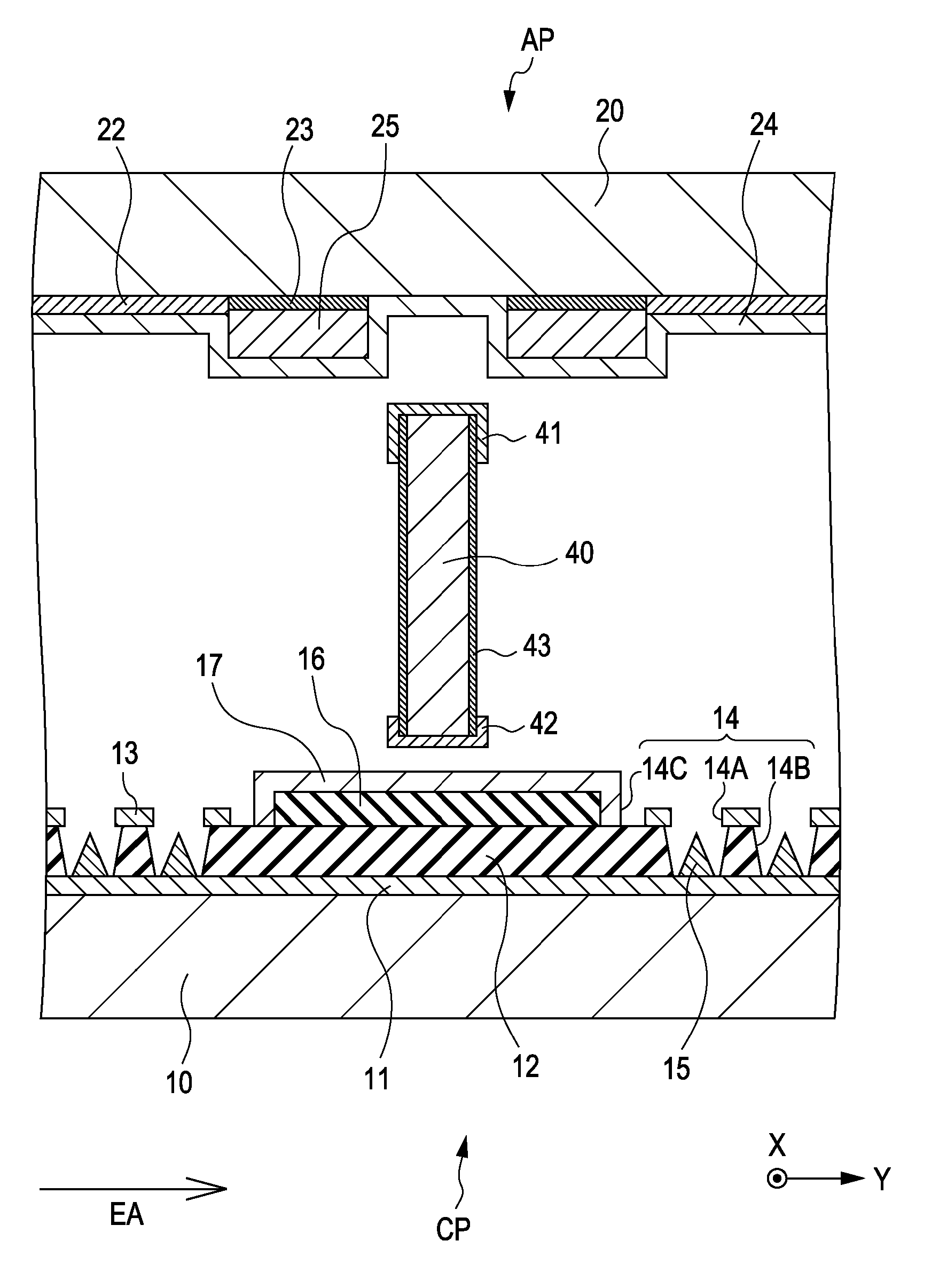
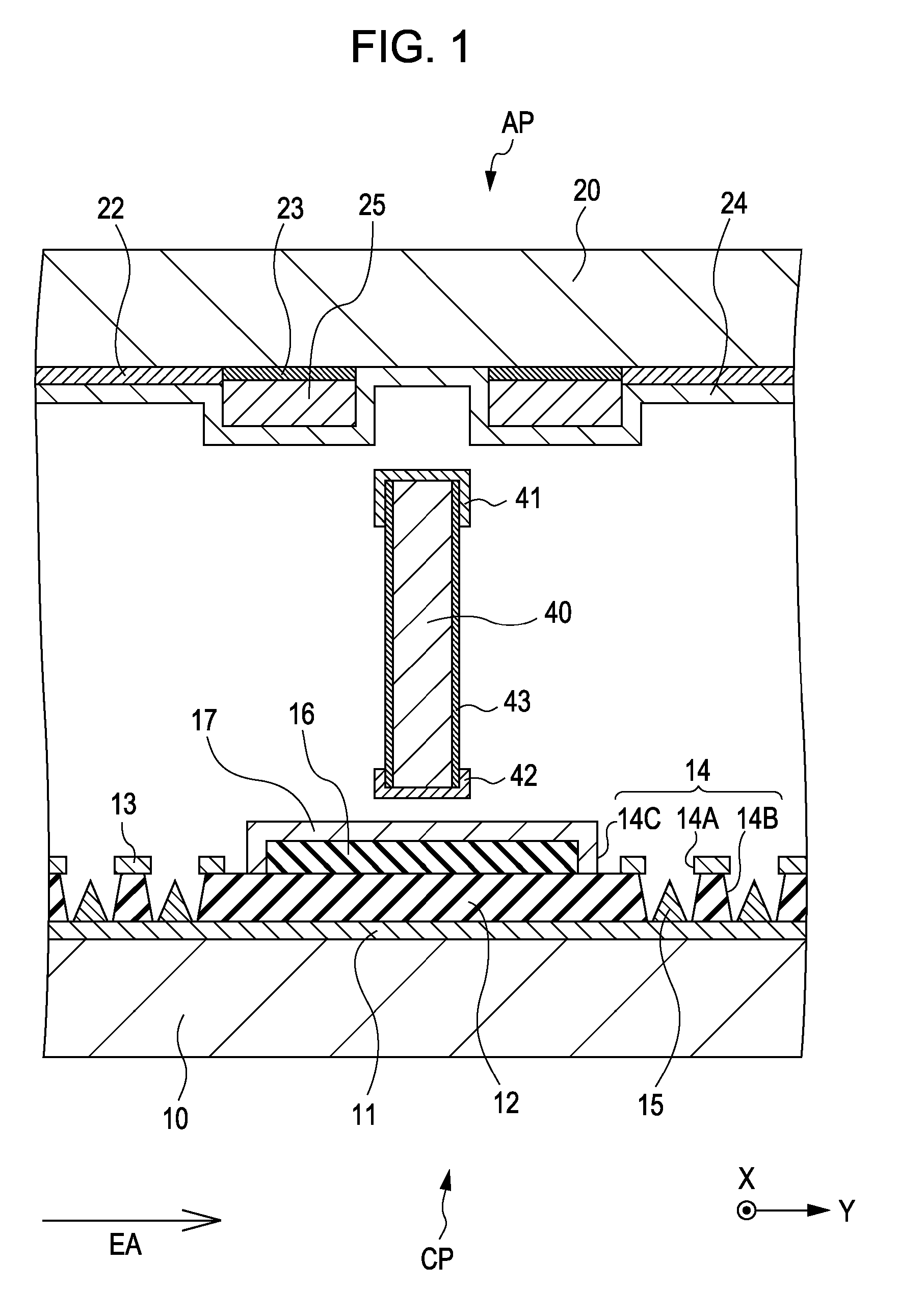
[0164] The second embodiment is a modification of the first embodiment. FIG. 3 is an enlarged schematic partial end view (exploded view) showing the vicinity of a spacer. In the second embodiment, a high-resistance layer 51 is formed on a portion of the anode panel AP which contacts each spacer 40. Specifically, the high-resistance layer 51 is formed on a portion of the anode panel AP which contacts each spacer 40 and more specifically formed on a portion of the anode electrode 24 which is disposed on the bottoms, sides, and tops of the spacer holding parts 25. The high-resistance layer 51 is composed of a SiC film of 0.2 μm in thickness and is formed by RF sputtering. The contact resistance between the high-resistance layer 51 and each spacer 40 is about 0.33×10⁹ Ω, and the sheet resistivity of the high-resistance layer 51 is about 0.33×10⁴ Ω·m2. The voltage applied in measurement is 1 kV.

[0165] The constitution, structure, and assembling method of the display according to the sec...

third embodiment

[0166] The third embodiment is also a modification of the first embodiment. FIG. 4 is an enlarged schematic partial end view (exploded view) showing the vicinity of a spacer. In the third embodiment, a high-resistance layer 51 is formed on a portion of a substrate constituting an anode panel.

[0167] More specifically, in the flat-panel display according to the third embodiment, the anode electrode 24 includes a plurality of anode electrode units 24A. The high-resistance layer 51 extends to the anode electrode units 24A and is electrically connected to the anode electrode units 24A.

[0168]FIG. 5 is a schematic view showing the arrangement of the anode electrode units 24A, the high-resistance layers 51, the partition walls 21, the spacer holding parts 25, the spacers 40, and the fluorescent layers 22 (22R, 22G, and 22B) on the anode panel AP constituting the flat-panel display of the third embodiment. FIG. 5 shows the partially cut-away spacers 40 for the convenience sake. As shown in...

fourth embodiment

[0173] The fourth embodiment is also a modification of the first embodiment. FIG. 7 is an enlarged schematic partial end view (exploded view) showing the vicinity of a spacer. In the fourth embodiment, a high-resistance layer includes a high-resistance member 61 held between the top surface of each spacer 40 and the anode electrode 24. More specifically, the high-resistance thin-plate member 61 is composed of high-resistance frit glass of several tens μm in thickness. In this case, the contact resistance of the high-resistance member 61 is about 0.33×10⁹ Ω, and the sheet resistivity of the high-resistance member 61 is about 0.33×10⁴ Ω·m2. The contact resistance or sheet resistivity of the high-resistance member 61 means the contact resistance or sheet resistivity between the anode electrode 24 and each spacer 40 with the high-resistance member 61 provided therebetween. The voltage applied in measurement is 1 kV.

[0174] The constitution, structure, and assembling method of the displa...


PUM


Abstract

A flat-panel display includes a cathode panel including a plurality of electron emission regions, and an anode panel including a fluorescent layer and an anode electrode, both panels being bonded together in a peripheral region and holding a vacuum space therebetween; a plurality of spacers disposed between the cathode panel and the anode panel; a high-resistance layer provided between the anode panel and each of the spacers; and a conductor layer provided on a portion of each of the spacers which contacts the cathode panel.

Description

CROSS REFERENCES TO RELATED APPLICATIONS [0001] The present invention contains subject matter related to Japanese Patent Application JP 2005-250823 filed in the Japanese Patent Office on Aug. 31, 2005 and Japanese Patent Application JP 2006-020840 filed in the Japanese Patent Office on Jan. 30, 2006, the entire contents of which are incorporated herein by reference. BACKGROUND OF THE INVENTION [0002] 1. Field of the Invention [0003] The present invention relates to a flat-panel display. [0004] 2. Description of the Related Art [0005] Various flat-panel displays have been investigated as image displays alternative to cathode ray tubes (CRT) which are now mainstream. Such flat-panel displays are exemplified by liquid crystal displays (LCD), electroluminescence displays (ELD), and plasma display panels (PDP). In addition, the development of flat-panel displays combined with electron emission devices has been advanced. Known examples of the electron emission devices include a cold-catho...

Claims


Application Information

Patent Timeline
Patent Type & Authority Applications(United States)
IPC IPC(8): H01J19/42H01J1/88
CPCH01J29/028H01J29/864H01J31/127H01J2329/864H01J2329/8665H01J2329/865H01J2329/8655H01J2329/866H01J2329/8645
Inventor SATA, HIROSHIOKANAN, SATOSHIHONDA, KEIJIKATO, YOSHIMITSUSEKI, ATSUSHI
Owner SONY CORP
Why Eureka
Try Eureka