Method and System for Performing Functional Formal Verification of Logic Circuits

a logic circuit and functional verification technology, applied in the field of logic circuit functional formal verification, can solve the problems of inherently difficult functional formal verification of a dput at the register-transfer level, enormous input signal value space cannot be completely verified by logic simulation, and the complexity of hardware designs of the day is much more complex

Inactive Publication Date: 2007-03-01
IBM CORP
View PDF5 Cites 44 Cited by
  • Summary
  • Abstract
  • Description
  • Claims
  • Application Information

AI Technical Summary

Benefits of technology

[0040] It is an advantage of the present invention that the complete error space can be covered for all types of fault models that can be used at the RTL. The number of errors per cycle can be user-defined. The number of detected design errors is used to determine the overall coverage in relation to the number of injected errors. In case the coverage is considered to be insufficient, additional error detection logic can be added to the logic design as compensation.
[0041] In a further advantage of the invention it is possible to detect even errors in the design specification. Especially, the invention enables the functional verification of unconsidered corner cases.

Problems solved by technology

But today's hardware designs are much more complex.
This enormous input signal value space cannot be verified by logic simulation completely.
But also functional formal verification of a DPUT at the register-transfer level is inherently difficult using automated methods.
Except for special cases, attempts to formally verify a DUT result in either memory (BDD-based algorithms) or runtime (SAT-based algorithms) explosions.
Sources of permanent faults are real physical defects caused by manufacturing faults, pollution or material weaknesses.
A disadvantage of this model is that it can only be simulated explicitly at the switch- or the transistor level.
A bridge may cause transistor stuck-close behavior fault due to a low-resistance bridge between source and drain.
Another possibility for permanent faults is the occurrence of dynamical effects like path delays.
A low-resistance causes often a delay or even a stuck-fault.
But a high-resistance bridge may cause negligible delays or exceptionally even a speed-up of signals.
Beyond permanent faults, integrated systems of recent years are more susceptible to temporary effects like transient and intermittent faults.
These errors are the major portion of digital system malfunctions, and have been found to account for more than 90% of the total maintenance expense.
But it is impossible to reproduce or to simulate all effects in advance that may occur during the lifetime on an embedded system.
The errors as a result of these faults are troublesome due to their potential for a system failure, and elude many current testing methods.
New faults emerge during the system life time or due to changed operation parameters.
Intermittent faults can occur due to partially defective components, loose connections.
Especially weak faults contain the risk of an error if they grow up to breaks or bridges.
In bad hardware designs a too small distance between lines (hardly bridge) injures defined layout rules.
It may cause steady but not regular recurred voltage breaks through the isolation material.
It may be blown like a fuse if a voltage difference between lines is exceeded.
For instance, a bridge between input and output causes different erroneous behavior.
Beyond recurrent path or gate delays (permanent delay) because of inadequate timing simulation, this effect can be caused by external influences or changing material characteristics.
Effective errors corrupt control and / or data flow with or without latency.
An error is a signal value other than the normal output of a properly operating circuit.
Especially, the error injection in logic design models can use fault models to emulate realistic faults.
But these changes may introduce unintended errors also.
They all share the disadvantage to be specific to a certain DUT, and a significant adaptation effort for new design development projects is needed.
The injection of multiple errors is rarely done since the number of different error combinations increases exponentially with the number of simultaneous errors, each combination requiring a separate logic simulation run.
However, this approach is also injecting irrelevant cases: Also a signal value will be injected that is already produced by the logic design.
Errors in a pipeline stage of a pipelined processor are difficult to detect since it can take many cycles until they have an effect to the operation of the processor.
Because of the huge state space even for a small number of pipeline stages it is difficult or even impossible to prove the correct behaviour of such ED logic in pipelined processor designs.
Design specifications for ED logic are often based on rules of thumb and logical considerations only and therefore incomplete.
A formal functional verification of a design against a design specification, however, cannot cover the errors in the design specification itself.

Method used


Image

  • Method and System for Performing Functional Formal Verification of Logic Circuits
  • Method and System for Performing Functional Formal Verification of Logic Circuits
  • Method and System for Performing Functional Formal Verification of Logic Circuits

Examples


Embodiment Construction

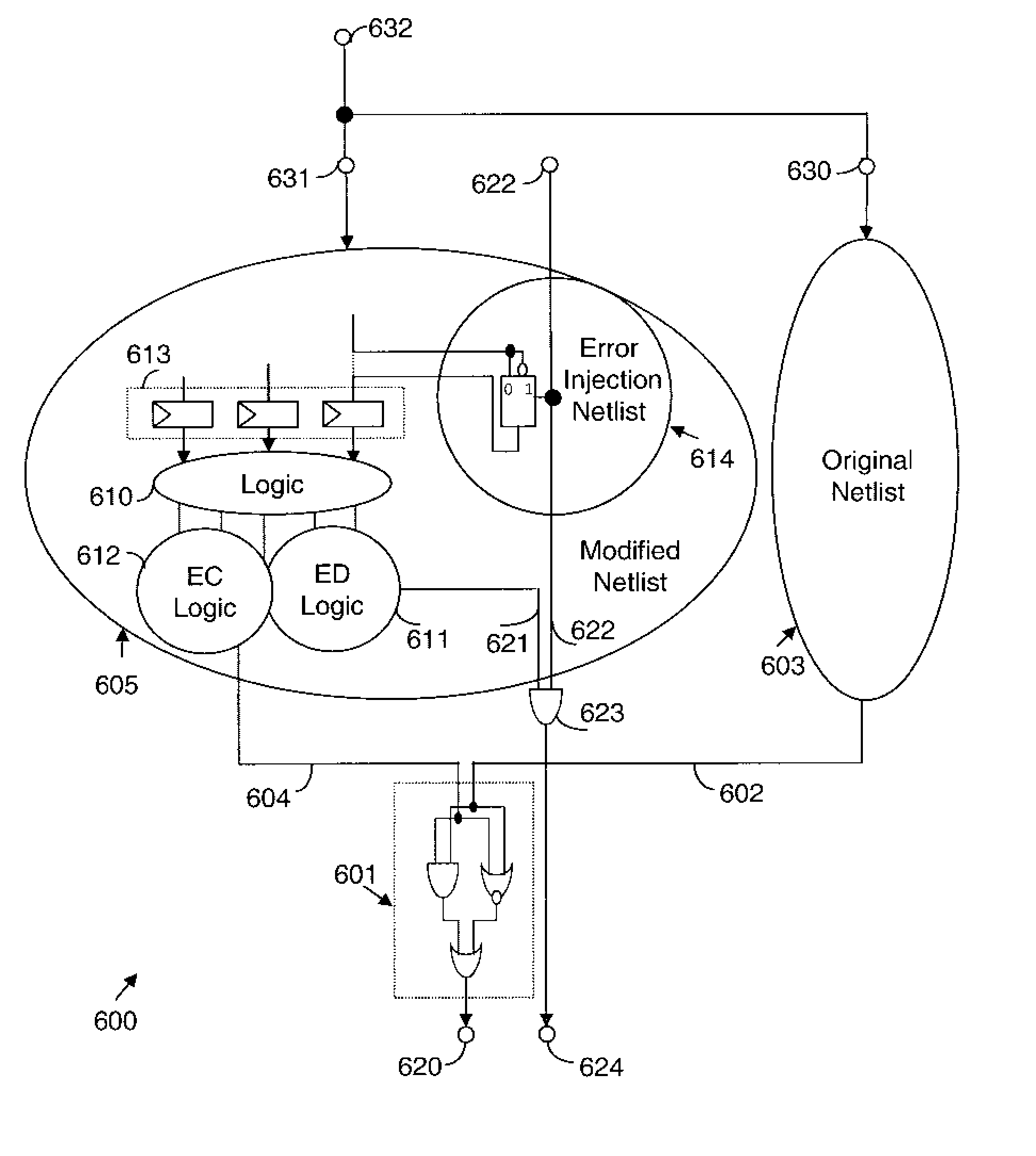
[0053] In the standard hardware design development processes the latches survive every automatic design transformation, for example a transformation from the RTL to the gate level using logic synthesis methods. In the preferred embodiment of the invention the injection of errors using fault models is performed at the RTL if an automatic transformation step from the RTL to the gate level is used, and the fault models are based on modifications of the latches. If no automatic transformation step from the RTL to the gate level is used in the hardware design development process, the error injection should be performed at the gate level in order to detect the errors introduced during the transformation step.

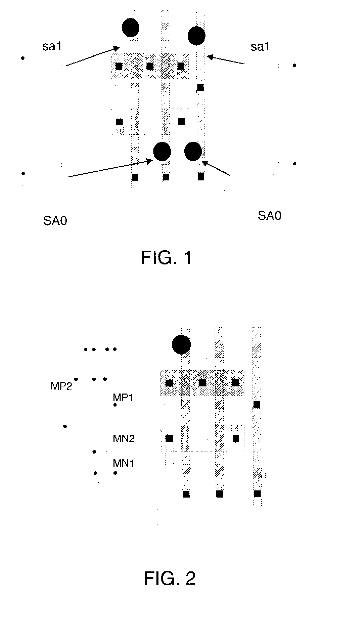
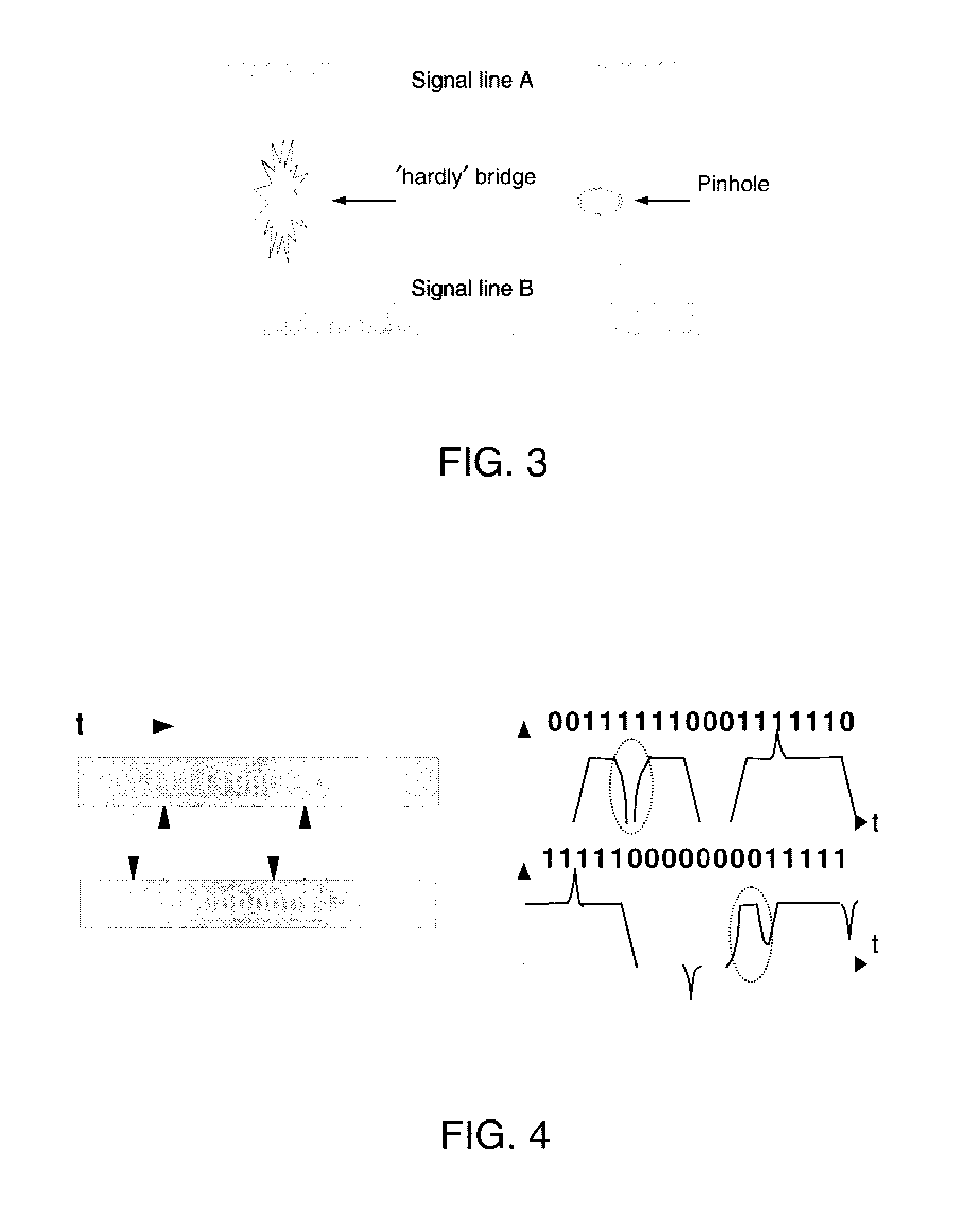
[0054] The injection of a permanent fault (e.g., stuck faults as in FIG. 1 and FIG. 2) can be done by simply switching a signal value. Examples for gate level models of transient faults (for example the faults in FIG. 3 and FIG. 4) in accordance with the present invention are given i...


PUM


Abstract

The present invention relates to a method, a computer program product and a system for performing functional formal verification. Error detection logic is verified by injecting errors in a hardware design description without any changes to the original design description. With the present invention both permanent and transient faults can be modelled, and the complete error space can be covered for all types of fault models that can be used at the RTL. The number of detected design errors is used to determine the overall coverage in relation to the number of injected errors. The error injection is prepared by adding additional circuits to an RTL netlist representation of the hardware logic design. Signal values for selected signals related to the error detection logic are compared for a modified netlist representation and for the original netlist using a formal verification tool.

Description

BACKGROUND OF THE INVENTION [0001] The present invention relates to a method, a system, and a computer program product for performing functional formal verification of logic circuits. Logic Design Verification [0002] Digital logic circuits implement a logic function and represent the core of any computer or processing unit. Thus, before a “logic design” is constructed in real hardware, it must be tested and the proper operation thereof has to be verified against the design specification. This task is called functional verification of a design under test (DUT) and described for example in J . M. Ludden et al.: “Functional verification of the POWER4 microprocessor and POWER4 multiprocessor systems”, IBM Journal of Research and Development, Vol. 46 No. 1, January 2002. [0003] The functional verification can be performed at various abstraction levels for the hardware design, e.g. the switch level and the transistor level. The switch level typically includes active circuit elements (e.g...

Claims


Application Information

Patent Timeline
Patent Type & Authority Applications(United States)
IPC IPC(8): G06F17/50
CPCG06F17/504G06F30/3323
Inventor JACOBI, CHRISTIANPARUTHI, VIRESHPFLANZ, MATTHIASWEBER, KAI
Owner IBM CORP
Why Eureka
Try Eureka