
Method and apparatus to produce single crystal ingot of uniform axial resistivity

a technology of axial resistivity and ingot, which is applied in the direction of polycrystalline material growth, crystal growth process, polycrystalline material growth, etc., can solve the problems of reducing the resistivity of boule, difficult to introduce granular material into high-temperature furnaces,

Inactive Publication Date: 2007-03-15
REXOR
View PDF9 Cites 48 Cited by
  • Summary
  • Abstract
  • Description
  • Claims
  • Application Information

AI Technical Summary

Benefits of technology

"The present invention provides a method and apparatus for producing a single crystal ingot with uniform resistivity (i.e., axial resistivity) from the top to the tail of the boule. The technical effects of this invention include overcoming limitations and disadvantages of the related art, achieving consistent resistivity along the length of the ingot, and improving the quality and efficiency of the production process."

Problems solved by technology

The Czochralski process is conducted batch-wise and inherent limitations of batch-wise processing cause, or promote, variations in properties and composition of the resulting silicon boule.
It is also difficult to introduce a granular material into a high temperature furnace at closely controlled feed rates, as required to avoid upsetting the process conditions within the furnace.
A common problem with all silicon crystal growth furnaces is the impossibility of obtaining a uniform distribution of the minor quantities of dopant throughout the polycrystalline silicon supplied to the furnace so that variations in dopant concentration are avoided in the melt and subsequently in the single crystal boule.
This results in incorporation of more dopant in the next crystallization phase, thereby increasing the dopant content in the crystal, thus, reducing the resistivity of the boule.

Method used


Image

  • Method and apparatus to produce single crystal ingot of uniform axial resistivity
  • Method and apparatus to produce single crystal ingot of uniform axial resistivity
  • Method and apparatus to produce single crystal ingot of uniform axial resistivity

Examples


Embodiment Construction

[0034] Reference will now be made in detail to the embodiments of the present invention, examples of which are illustrated in the accompanying drawings.

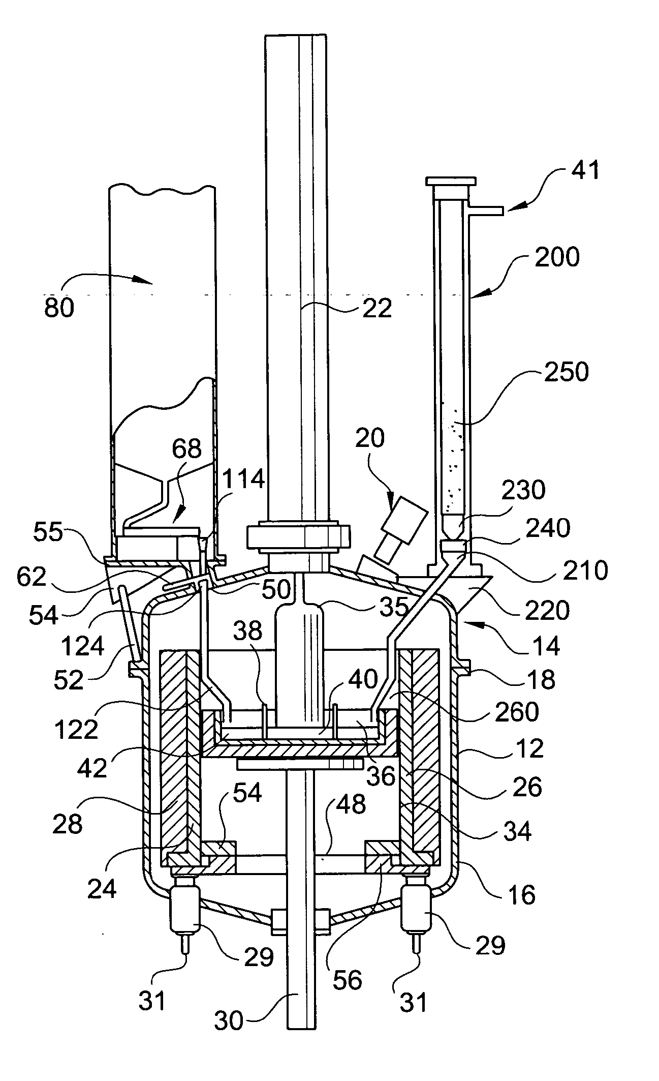
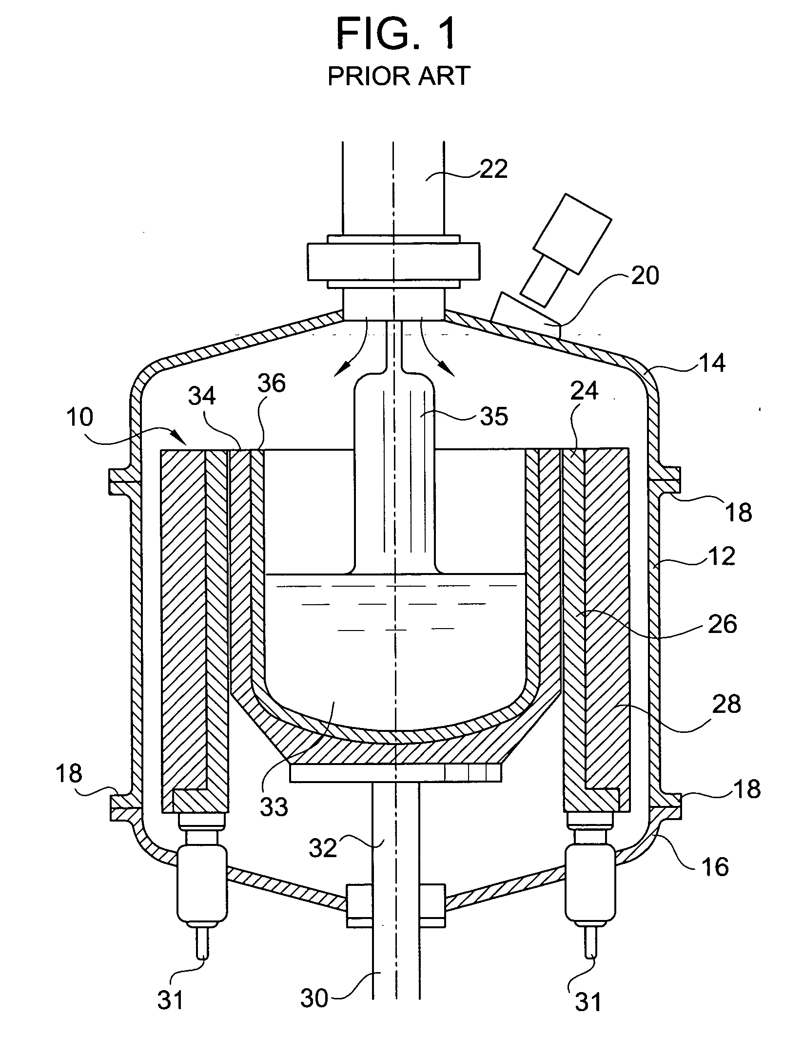
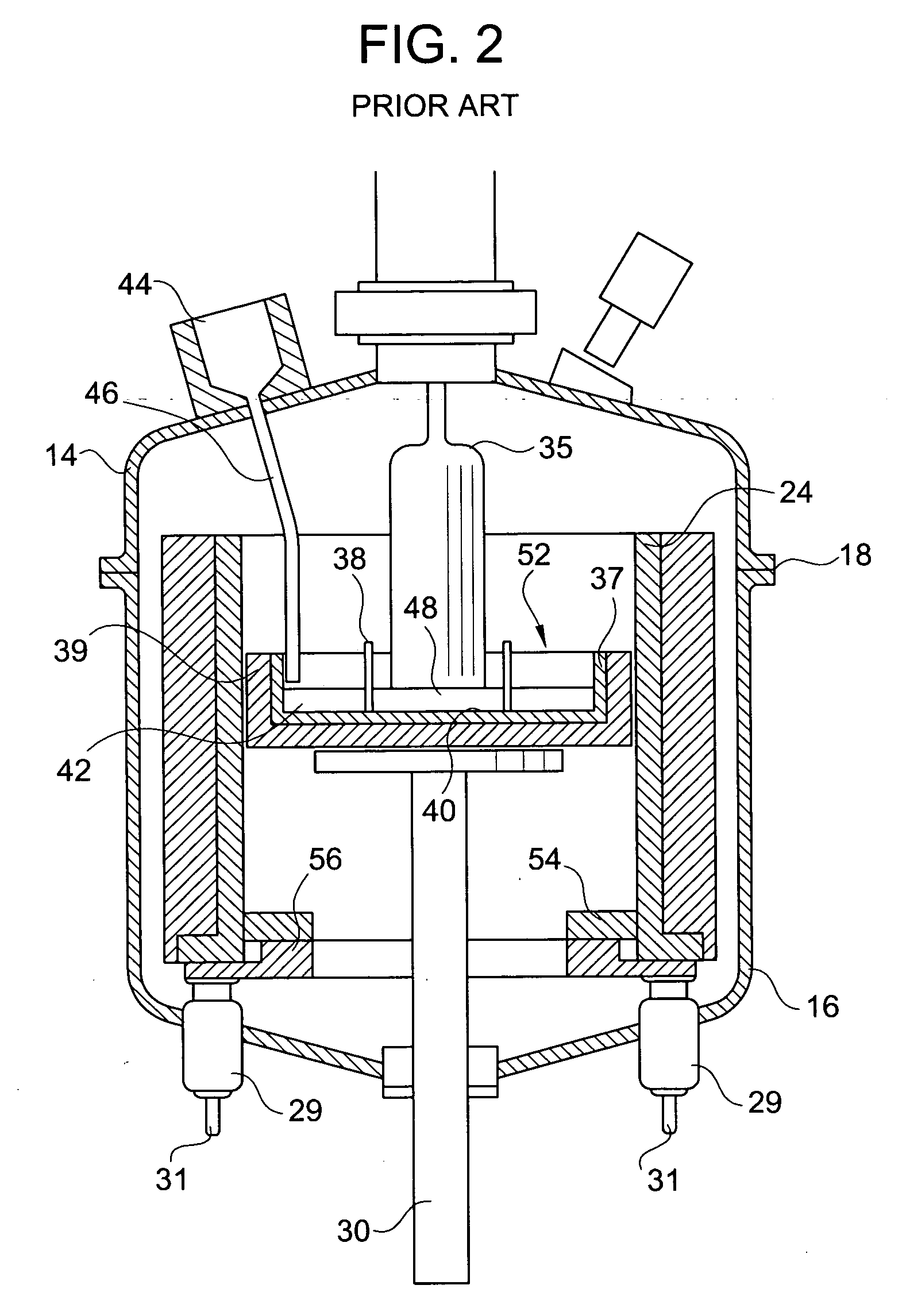
[0035]FIG. 3 is an elevation view of an exemplary modified Czochralski process furnace of one embodiment according to the present invention. In FIG. 3, a furnace 10 is contained within a surrounding vacuum chamber 12 formed from an upper half shell 14 and a lower half shell 16 which are joined together by annular flanges 18. Upper half shell 14 has a viewing port 20 and a centrally located, axially extending crystal receiving chamber 22. Vacuum chamber 12 contains a centrally located, furnace 10 which includes a circular heater 24 formed of vertical graphite elements which are supplied with electrical power from electrical leads 31 which pass into the chamber through connectors 29. Heater 24 is surrounded by a protective cylindrical heat shield 28.

[0036] A centrally located shaft 30 extends axially into the lower shell 16, and this...


PUM

PropertyMeasurementUnit
melt temperatureaaaaaaaaaa
average particle diameteraaaaaaaaaa
depthaaaaaaaaaa

Abstract

A method for producing a single crystal ingot includes steps of providing a first amount of polycrystalline material and a first amount of dopant material to form a first mixture having a first dopant concentration in a process furnace, increasing a temperature of the first mixture to provide a molten first mixture, providing a seed material to the molten first mixture, withdrawing the seed from the molten first mixture by a first distance to form a boule having a first length, providing a second amount of the polycrystalline material and a second amount of the dopant material to the molten first mixture to provide a molten second mixture having the first dopant concentration, withdrawing the first length of the boule from the molten second mixture by a second distance to form the boule having a second length, and removing the boule from the molten second mixture to form the single crystal ingot of uniform axial resistivity.

Description

BACKGROUND OF THE INVENTION [0001] 1. Field of Invention [0002] The present invention relates to a method and apparatus for producing single crystal material and, in particular, to a method and apparatus for producing single crystal ingot of uniform axial resistivity. [0003] 2. Discussion of the Related Art [0004] Single crystal silicon, Group IV element, is the basic substance used for virtually all semiconductor devices. Other single crystal materials which are also finding applications in semiconductor devices are Periodic Table Group III elements, particularly in combination with Group V elements, e.g., germanium and gallium arsenide. These materials are synthetically produced in a purified and perfect, single crystal form. The method traditionally used for such production has been the Czochralski method. In the Czochralski method, polycrystalline material, such as hyper-pure germanium or silicon, is melted and maintained in a molten state in a quartz crucible. The quartz crucib...

Claims


Application Information

Patent Timeline
Patent Type & Authority Applications(United States)
IPC IPC(8): C30B15/00C30B21/06C30B27/02C30B28/10C30B30/04
CPCC30B15/04C30B35/00C30B15/12
Inventor LIM, JOHN C.
Owner REXOR
Learn More