Silicon-on-insulator (SOI) read only memory (ROM) array and method of making a soi ROM

a technology of silicon-on-insulator and read-only memory, which is applied in the direction of diodes, semiconductor devices, electrical apparatus, etc., can solve the problems of large voltage drop of diode current flowing through this resistance, inability to achieve discrete diodes in bulk silicon, and inability to achieve soi rom cell efficiency, etc., to achieve the effect of minimizing rom cell signal loss, increasing soi ic on-chip rom density, and increasing rom density

Inactive Publication Date: 2007-03-15
GLOBALFOUNDRIES INC
View PDF8 Cites 59 Cited by
  • Summary
  • Abstract
  • Description
  • Claims
  • Application Information

AI Technical Summary

Benefits of technology

[0011] It is another purpose of the invention to increase ROM density in Silicon-on-insulator (SOI) Integrated Circuits (ICs) while minimizing ROM cell signal loss;
[0012] It is yet another purpose of the invention to increase SOI IC on-chip ROM density to minimum line pitch for surface silicon layer lines without significantly complicating chip manufacturing.

Problems solved by technology

Diodes have not proven very efficient for SOI ROM cells.
Discrete diodes are impractical in bulk silicon because active devices, including diodes, share the bulk substrate in common, i.e., transistor collectors / FET substrates are in the same shared diode terminal (anode / cathode).
Moreover, when the maximum available voltage is limited (currently to approximately 1 Volt), the voltage dropped by diode current flowing through this resistance can absorb a large percentage of the available signal.
Conventional saliciding of the silicon strip to reduce resistance tends to short the surface electrodes together, frustrating individual diode formation.

Method used


Image

  • Silicon-on-insulator (SOI) read only memory (ROM) array and method of making a soi ROM
  • Silicon-on-insulator (SOI) read only memory (ROM) array and method of making a soi ROM
  • Silicon-on-insulator (SOI) read only memory (ROM) array and method of making a soi ROM

Examples


Embodiment Construction

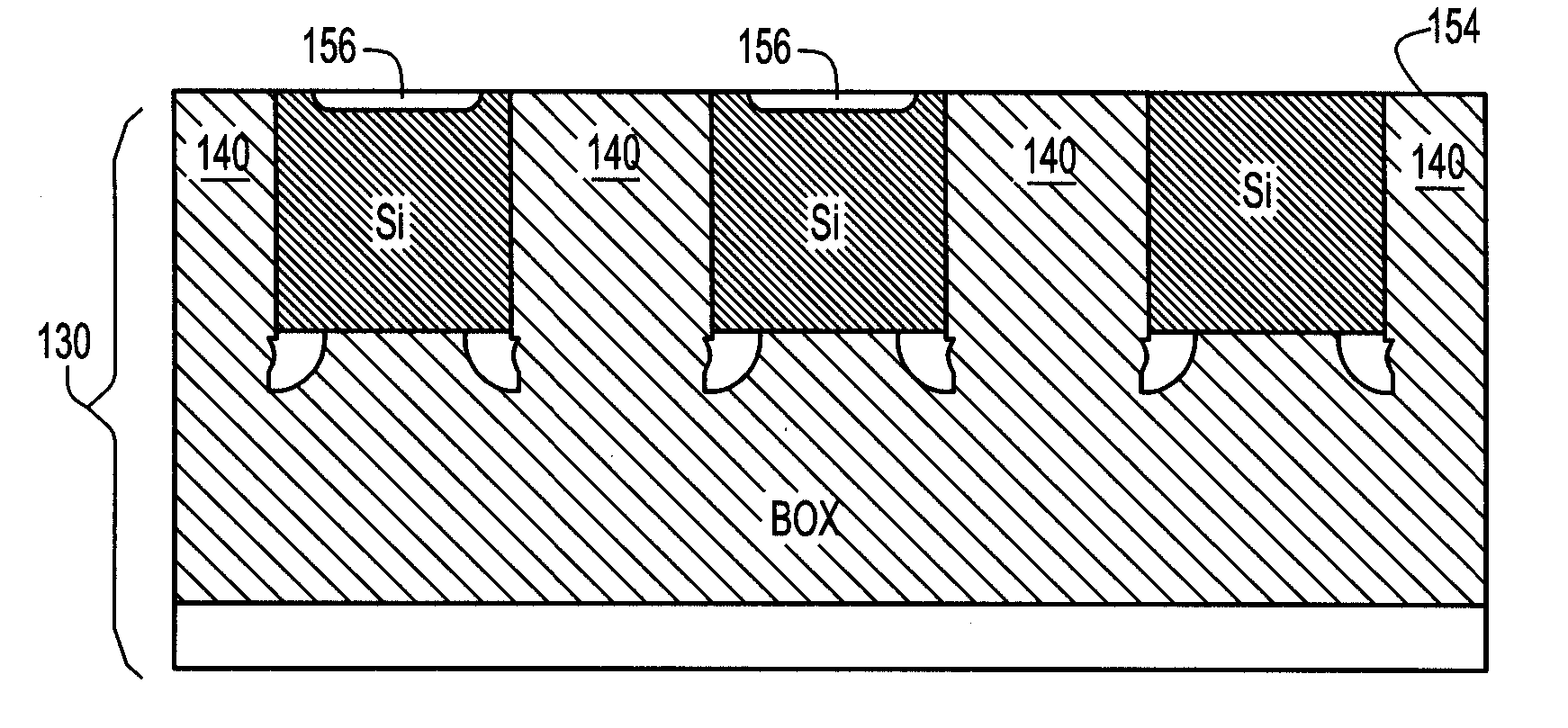
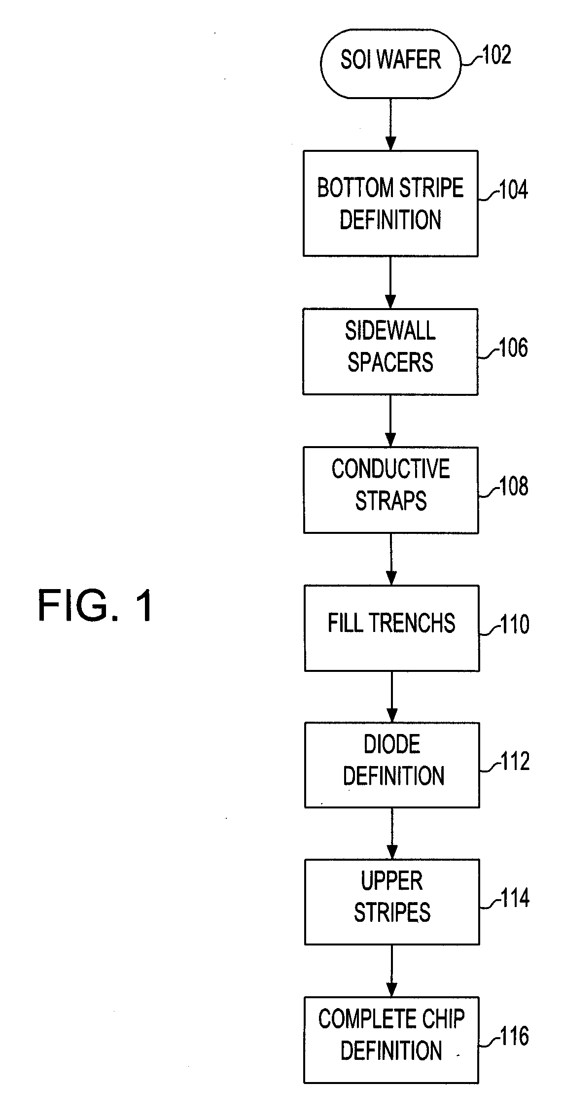
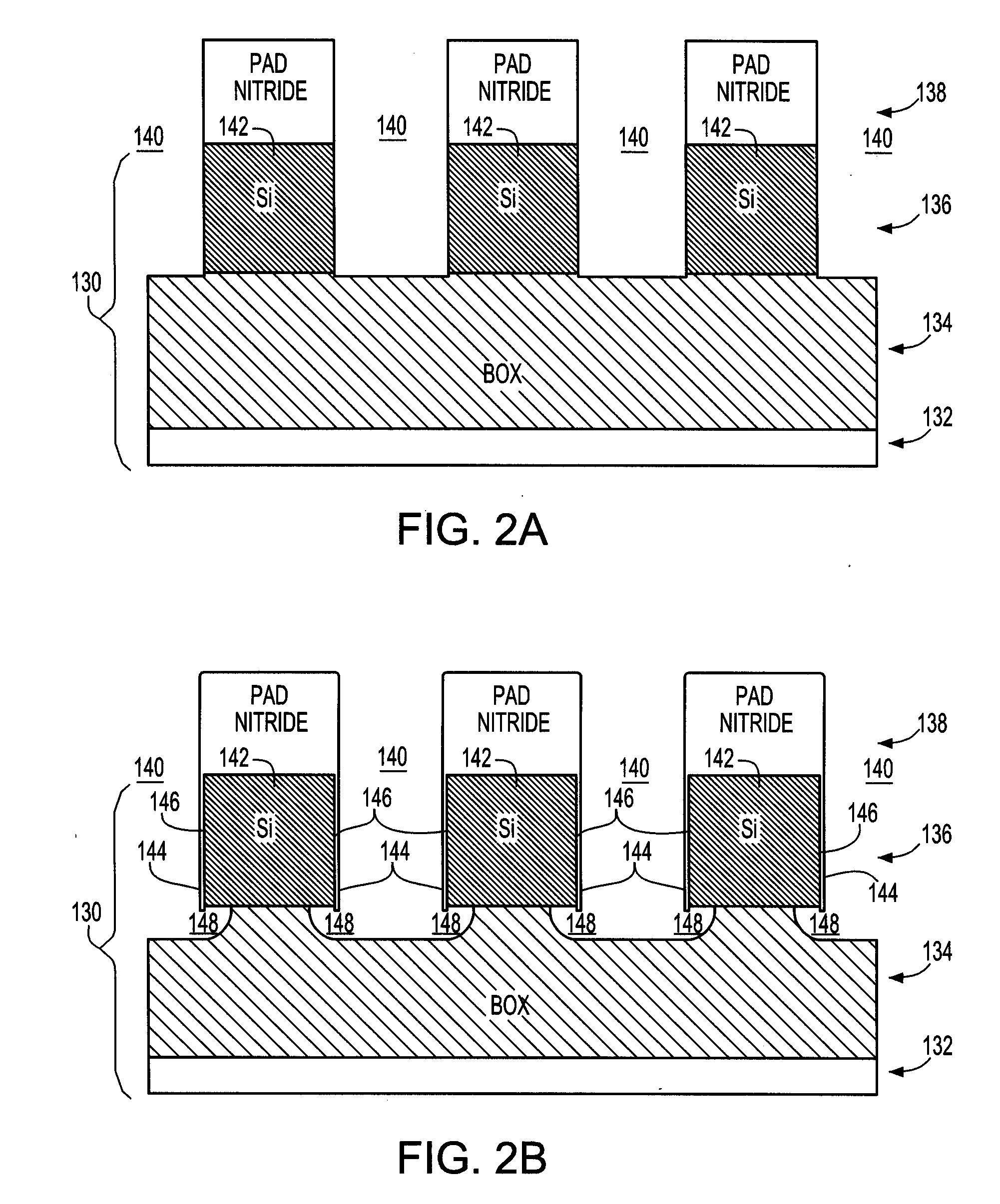
[0020] Turning now to the drawings more particularly FIG. 1 shows a flow diagram example of steps in forming an array of Read Only Memory (ROM) cells, e.g., a cross point ROM array, according to a preferred embodiment of the present invention. Preferably, the array is formed in a standard Silicon-on-insulator (SOI) wafer 102, and includes a pair of layers of orthogonal conductive lines with each cell selectively including a diode and connection to lines in the orthogonal layers. The diodes are vertical diodes all oriented in the same direction, e.g., each with its cathode at a conductive line in the first layer (e.g., the silicon surface layer) and its anode selectively connected to a conductive line in the other layer, e.g., an overlying wiring layer. Thus, for example, by placing a voltage on a line in the upper conductive layer, a voltage sufficient to bias connected diodes above the turn-on (˜0.7V), diodes connected to the line turn on and conduct. The conducting diodes pass cur...


PUM


Abstract

A silicon-on-insulator (SOI) Read Only Memory (ROM), and a method of making the SOI ROM. ROM cells are located at the intersections of stripes in the surface SOI layer with orthogonally oriented wires on a conductor layer. Contacts from the wires connect to ROM cell diodes in the upper surface of the stripes. ROM cell personalization is the presence or absence of a diode and/or contact.

Description

BACKGROUND OF THE INVENTION [0001] 1. Field of the Invention [0002] The present invention is related to nonvolatile storage and more particularly to integrated circuit chips including nonvolatile storage such as one or more cells or an array of nonvolatile random access memory (NVRAM) cells. [0003] 2. Background Description [0004] Semiconductor memories made in well known complementary, insulated-gate Field Effect Transistor (FET) technology, commonly referred to as CMOS, are well known in the art. A typical semiconductor memory is an array of memory cells arranged in rows and columns. Each cell is addressed by coincidence of a row with a column. When each row is selected, e.g., driving a word line, cells in the row are connected to the respective column or bit lines. So, cells may be accessed by selecting a row, and checking for a signal response on one or more columns. [0005] In what is well known as a Read Only Memory (ROM), each ROM cell has fixed contents that may not be change...

Claims


Application Information

Patent Timeline
Patent Type & Authority Applications(United States)
IPC IPC(8): H01L27/12
CPCH01L27/1021H01L27/1203H01L27/11213H01L27/112H10B20/27H10B20/00
Inventor FURUKAWA, TOSHIHARUHAKEY, MARK C.HOLMES, STEVEN J.HORAK, DAVID V.KOBURGER, CHARLES W. IIIMANDELMAN, JACK A.
Owner GLOBALFOUNDRIES INC
Why Eureka
Try Eureka