

Method for producing a field effect semiconductor device
- Summary
- Abstract
- Description
- Claims
- Application Information
AI Technical Summary
Benefits of technology
Problems solved by technology
Method used
Image

Examples
embodiments
[0050] Hereinbelow, preferred embodiments of the present invention will be described with reference to the accompanying drawings.
example 1
[0051] Single-wall carbon nanotubes (SWNTs) were prepared by a laser ablation process using a carbon target containing Ni / Co respectively at 0.6 at %. The temperature for the preparation was 1,200 degrees. The SWNTs prepared were purified successively using aqueous hydrogen peroxide, hydrochloric acid, and an aqueous NaOH solution (M. Shiraishi et al. CPL 358 (2002), 213). Compositional analysis using an electron microscope and EDX, Raman spectroscopy, or the like confirmed that the SWNTs purified had a purity of 95% or more.
[0052] The thus obtained SWNTs were dispersed in a dimethylformamide (DMF) solution using ultrasonic waves for 2 hours, and then subjected to centrifugal separation by means of a centrifugal separator (at 4,000 rpm for 15 minutes) to obtain a dispersion liquid composed only of the supernatant in which the SWNTs were well dispersed.
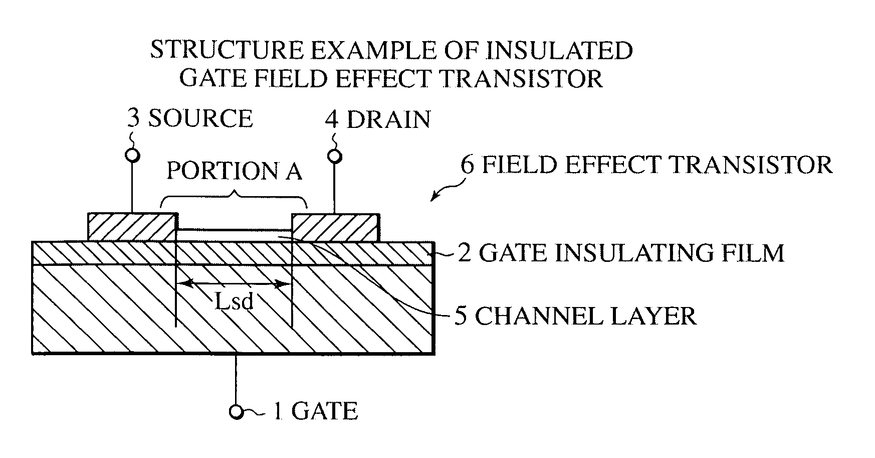
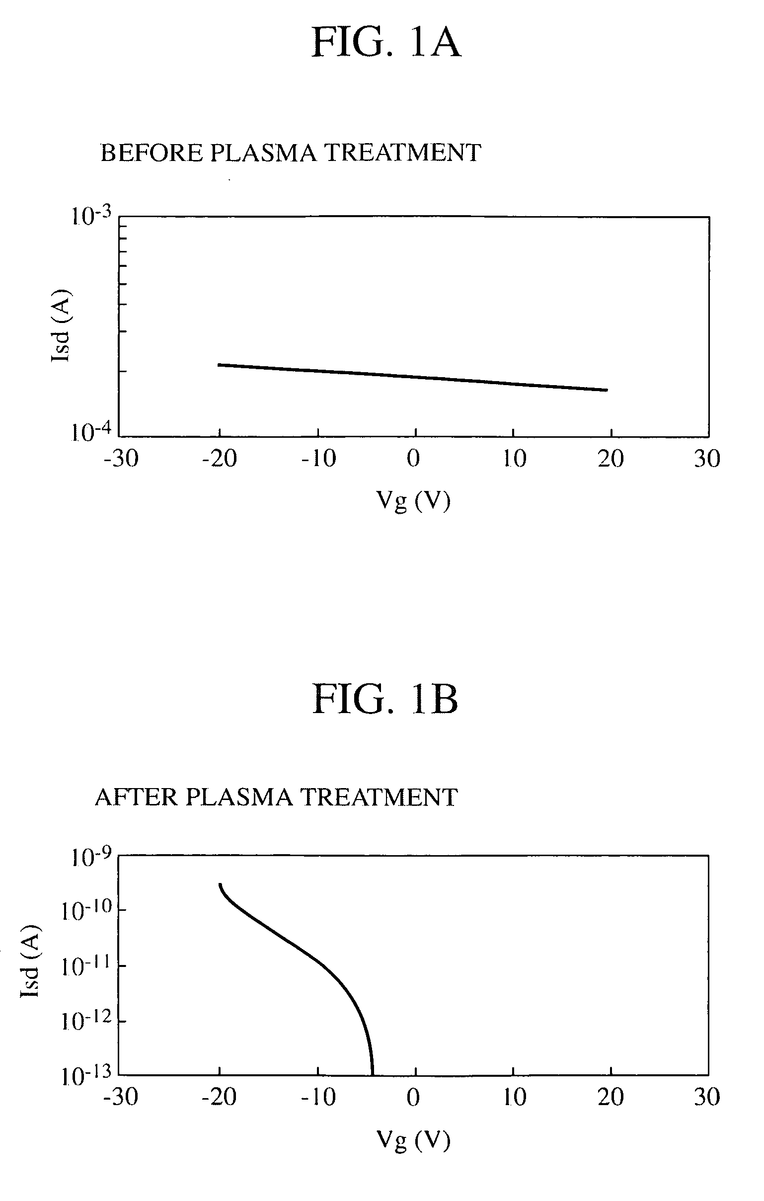
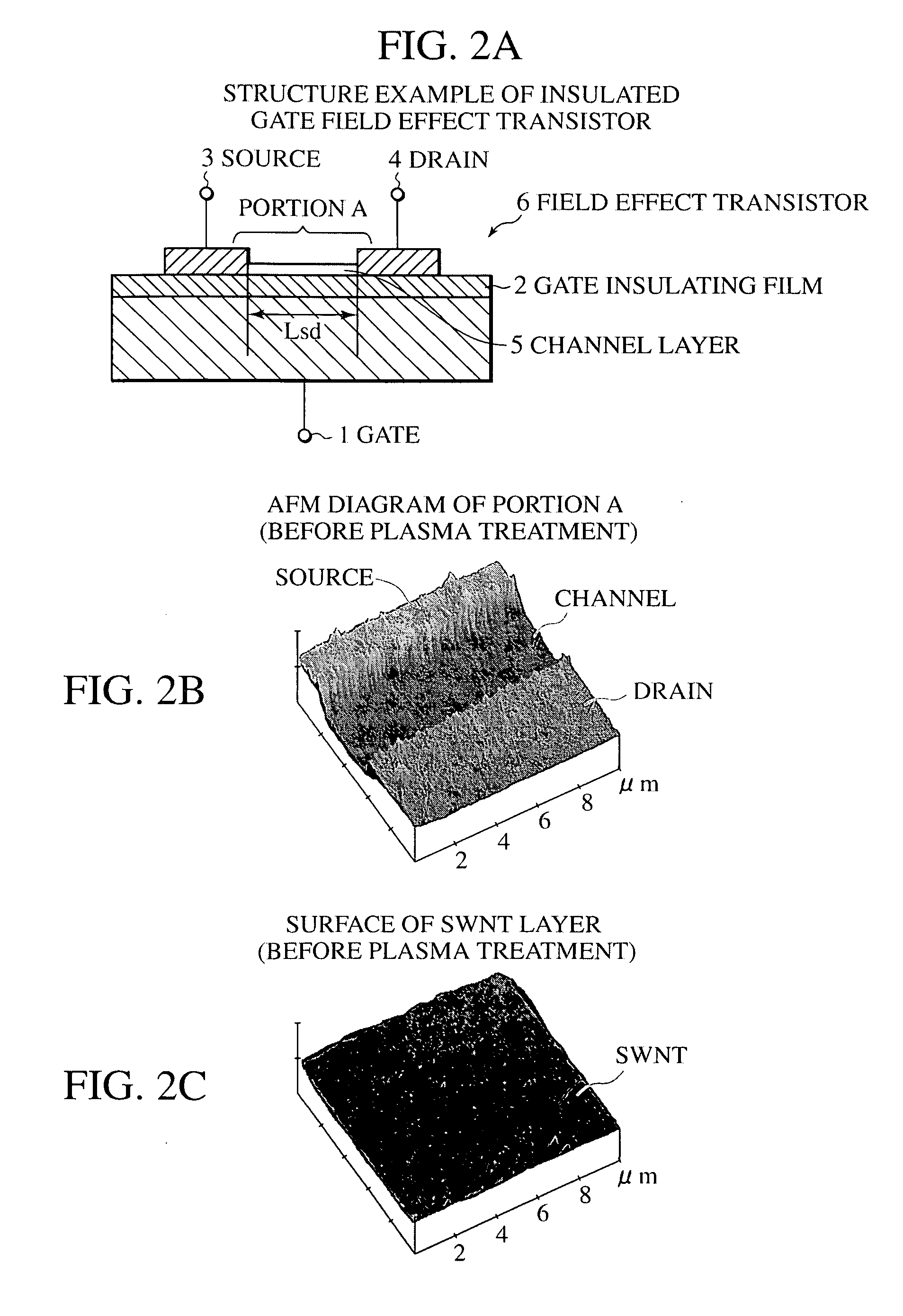
[0053] Then, the resultant dispersion liquid was applied dropwise to an SiO2 / Si substrate {electrode Fe / Au=10 / 200 nm; gate width (L...
example 2
[0062] Single-wall carbon nanotubes (SWNTs) were prepared by a laser ablation process using a carbon target containing Ni / Co respectively at 0.6 at %. The temperature for the preparation was 1,200 degrees. The SWNTs prepared were purified successively using aqueous hydrogen peroxide, hydrochloric acid, and an aqueous NaOH solution (M. Shiraishi et al. CPL 358 (2002), 213). Compositional analysis using an electron microscope and EDX, Raman spectroscopy, or the like confirmed that the SWNTs purified had a purity of 95% or more.
[0063] The thus obtained SWNTs were dispersed in a dimethylformamide (DMF) solution using ultrasonic waves for 2 hours, and then subjected to centrifugal separation by means of a centrifugal separator (at 4,000 rpm for 15 minutes) to extract only the well dispersed SWNT in the supernatant.
[0064] Then, the resultant dispersion liquid was applied dropwise to an SiO2 / Si substrate (electrode Fe / Au=10 / 200 nm; gate width (Lsd): 20 μm; gate length (w): 330 μm; oxide ...
PUM
 Abstract
Description
Claims
Application Information