Cleaved silicon substrate active device

a silicon substrate and active device technology, applied in the field of integrated circuit (ic) fabrication, can solve the problems of insufficient capability to realize some sophisticated functions such as cpu operations, the steady drive current produced by poly-si tfts is unlikely to be sufficient, and the stability of drive current produced by poly-si tfts may be inadequate for new technologies such as organic electroluminescent displays, so as to reduce the extent of p-dopant deactivation, reduce the level level level level level level level

Inactive Publication Date: 2007-03-22
SHARP KK
View PDF10 Cites 13 Cited by
  • Summary
  • Abstract
  • Description
  • Claims
  • Application Information

AI Technical Summary

Benefits of technology

[0013] This application addresses the problems associated with presence of hydrogen that may remain as a result of the substrate cleaving process. The problem is solved by implanting a region of p-dopant near the active regions, to act as a hydrogen gettering layer. Furthermore, any hydrogen in the channel region due to implantation, though at a lower concentration than at the cleaving plane, is also gettered by p-dopant near the S/D regions. As such, the hydrogen concentration in the channel is lower than in other regions where p-dopant is implanted. The decreased level of hydrogen in these areas reduces the extent of p-dopant deactivation.
[0014] Accordingly, a hydrogen (H) exfoliation gettering method is provided for attaching fabricated circuits to receiver substrates. The method comprises: providing a Si substrate; forming a Si active layer overlying the substrate with circuit S/D regions; implanting a p-dopant into the S/D regions; forming p-d...

Problems solved by technology

Unfortunately, this approach remains relatively expensive, even years after being introduced to LCD production.
Moreover, even if polysilicon thin film transistors (TFTs) can be efficiently produced using this method, it is unlikely that they have sufficient capability to realize some sophisticated functions like CPU operations, digital driver LCDC, digital-to-analog converter (DAC), memory, graphical controller, wireless, MPU, and digital signal processing.
Finally, the steadiness of drive currents produced by poly-Si TFTs may be inadequate for new technologies such organic electroluminescent displays.
There are two major problems that prevent the integration of the above-mentioned functions into integrated LCD products.
One is the film quality, and the other is the design limitations associated with glass substrates.
Each grain is oriented differently and surrounded by grain boundaries, which cause degradation in the resultant device characteristics.
Further, the poly-Si TFT device characteristics are not uniform.
The problem with the small, non-uniform grain size is compounded by the fact the energy-producing operations that can address this problem are limited by the sensitivity of LCD substrates to high temperatures.
In short, the convolution between cost and performance of polysilicon devices still pales compared to that o...

Method used


Image

  • Cleaved silicon substrate active device
  • Cleaved silicon substrate active device
  • Cleaved silicon substrate active device

Examples


Embodiment Construction

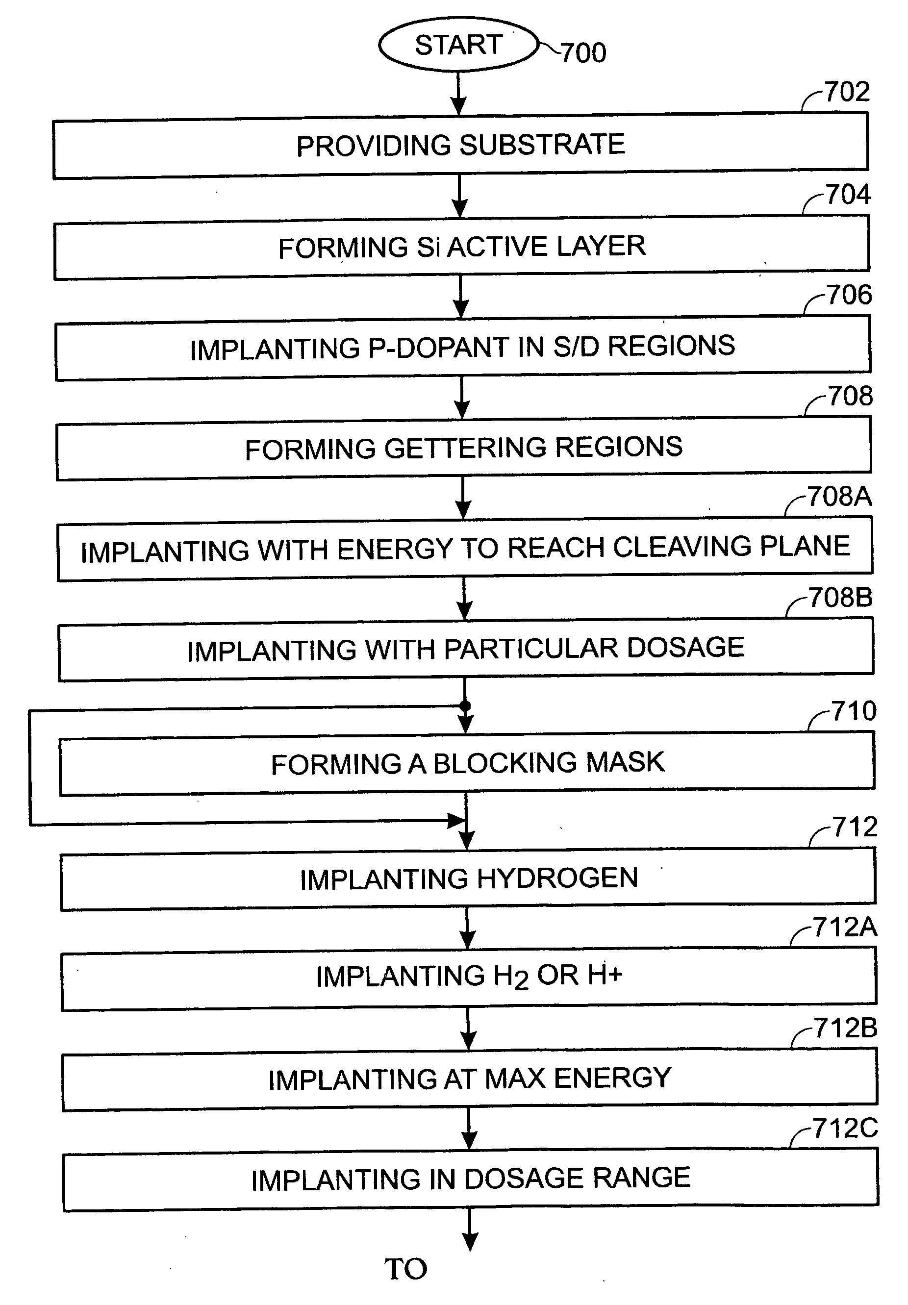
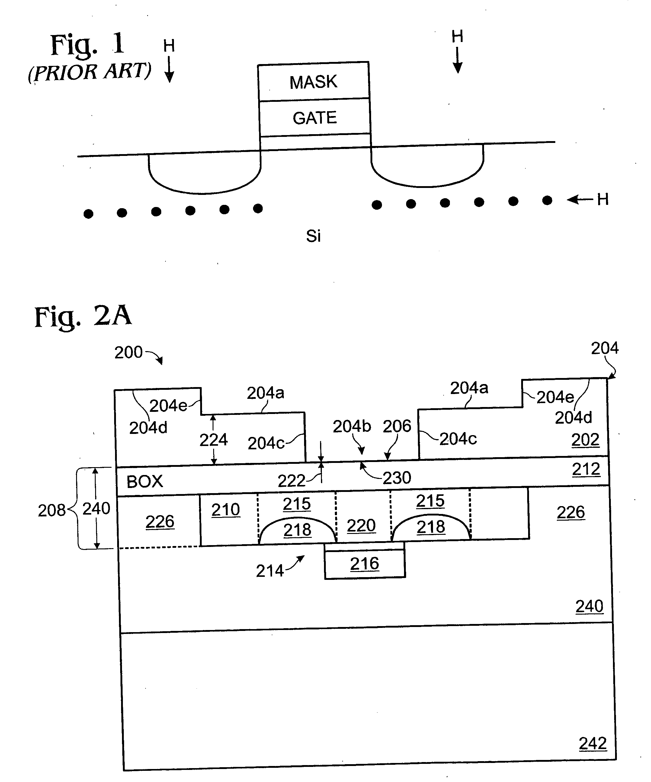
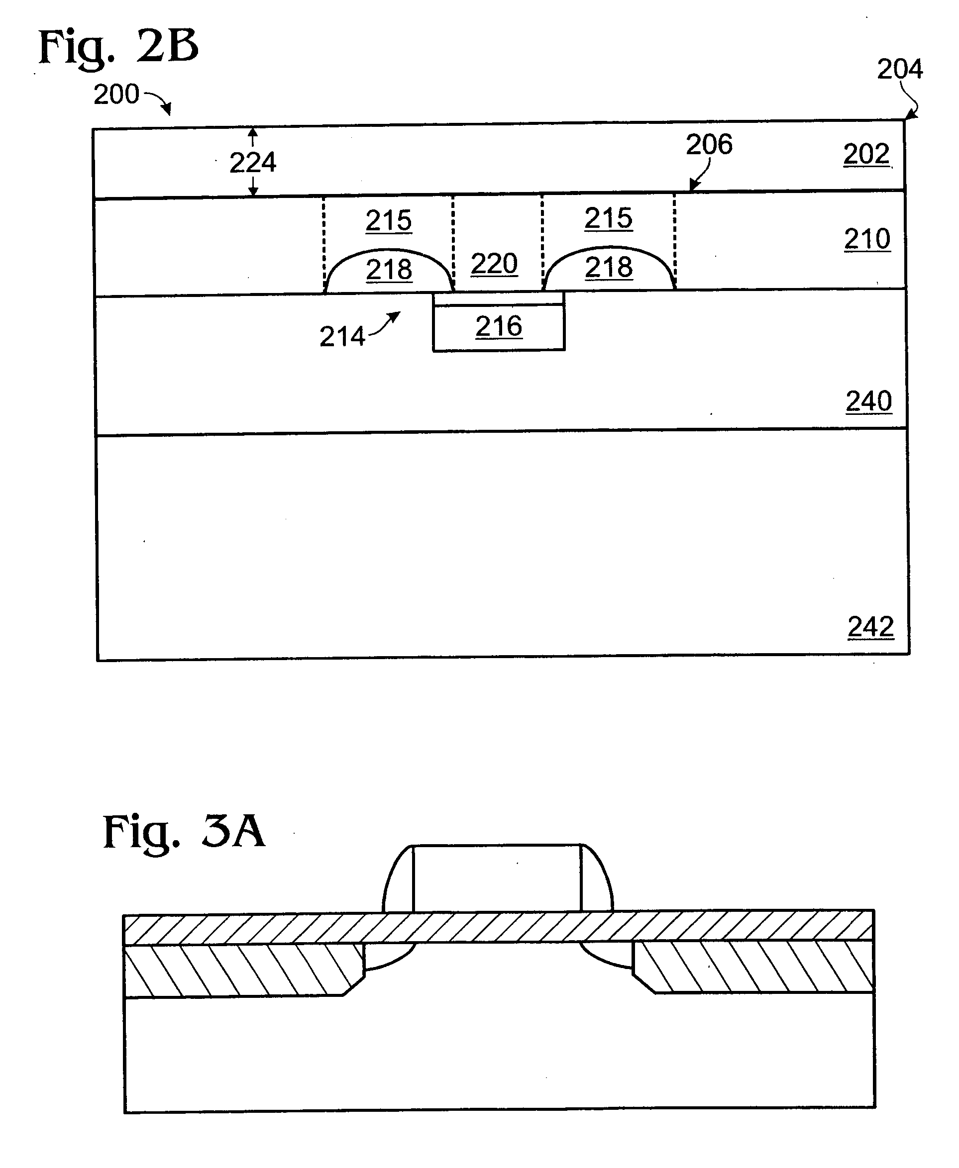
[0023]FIG. 2A is a partial cross-sectional view of an active Si device cleaved from a silicon-on-insulator (SOI) substrate. The active Si device 200 comprises a Si substrate 202 with a cleaving plane surface 204 and a bottom surface 206. A SOI substrate 208 includes a buried oxide layer (BOX) between a Si active layer 210 and Si substrate bottom surface 206. A circuit 214 is formed in the Si active layer 210. P-dopant gettering regions 215, referred to herein as gettering regions, are formed in the Si active layer 210, underlying the S / D regions. As shown, the circuit 214 in the Si active area 210 is a transistor or TFT. The TFT 214 includes a gate 216, channel region 220, and source / drain (S / D) regions 218 adjacent the channel region 220. Alternately but not shown, the circuit 214 in the Si active layer 210 can be any CMOS circuit or VLSI device (with many TFT or CMOS circuits) using a p-doped semiconductor material.

[0024] The Si substrate cleaving plane surface 204 includes a fir...


PUM


Abstract

A hydrogen (H) exfoliation gettering method is provided for attaching fabricated circuits to receiver substrates. The method comprises: providing a Si substrate; forming a Si active layer overlying the substrate with circuit source/drain (S/D) regions; implanting a p-dopant into the S/D regions; forming gettering regions underling the S/D regions; implanting H in the Si substrate, forming a cleaving plane (peak concentration (Rp) H layer) in the Si substrate about as deep as the gettering regions; bonding the circuit to a receiver substrate; cleaving the Si substrate along the cleaving plane; and binding the implanted H underlying the S/D regions with p-dopant in the gettering regions, as a result of post-bond annealing.

Description

RELATED APPLICATIONS [0001] This application is a Divisional Application of a patent application entitled, SYSTEM AND METHOD FOR HYDROGEN EXPOLIATION GETTERING, invented by Droes et al., Ser. No. 10 / 991,120, filed Nov. 16, 2004, which is a continuation-in-part of a pending application entitled SYSTEM AND METHOD FOR HYDROGEN EXFOLIATION, invented by Droes et al, filed on Sep. 29, 2004, Ser. No. 10 / 953,938, both of which are incorporated herein by reference.BACKGROUND OF THE INVENTION [0002] 1. Field of the Invention [0003] This invention generally relates to integrated circuit (IC) fabrication and, more particularly, to a method for transferring partially completed circuits from silicon substrates, to temperature sensitive substrates, for liquid crystal display (LCD) applications. [0004] 2. Description of the Related Art [0005] There is broad agreement in the flat panel display (FPD) industry that system-on-glass (SOG) technology is a natural evolutionary step for flat panel displays...

Claims


Application Information

Patent Timeline
IPC IPC(8): H01L21/322
CPCH01L21/26506H01L21/3221H01L27/1266H01L29/66772H01L29/78603H01L21/76254H01L21/26513
Inventor DROES, STEVEN R.TAKAFUJI, YUTAKA
Owner SHARP KK
Why Eureka
Try Eureka