

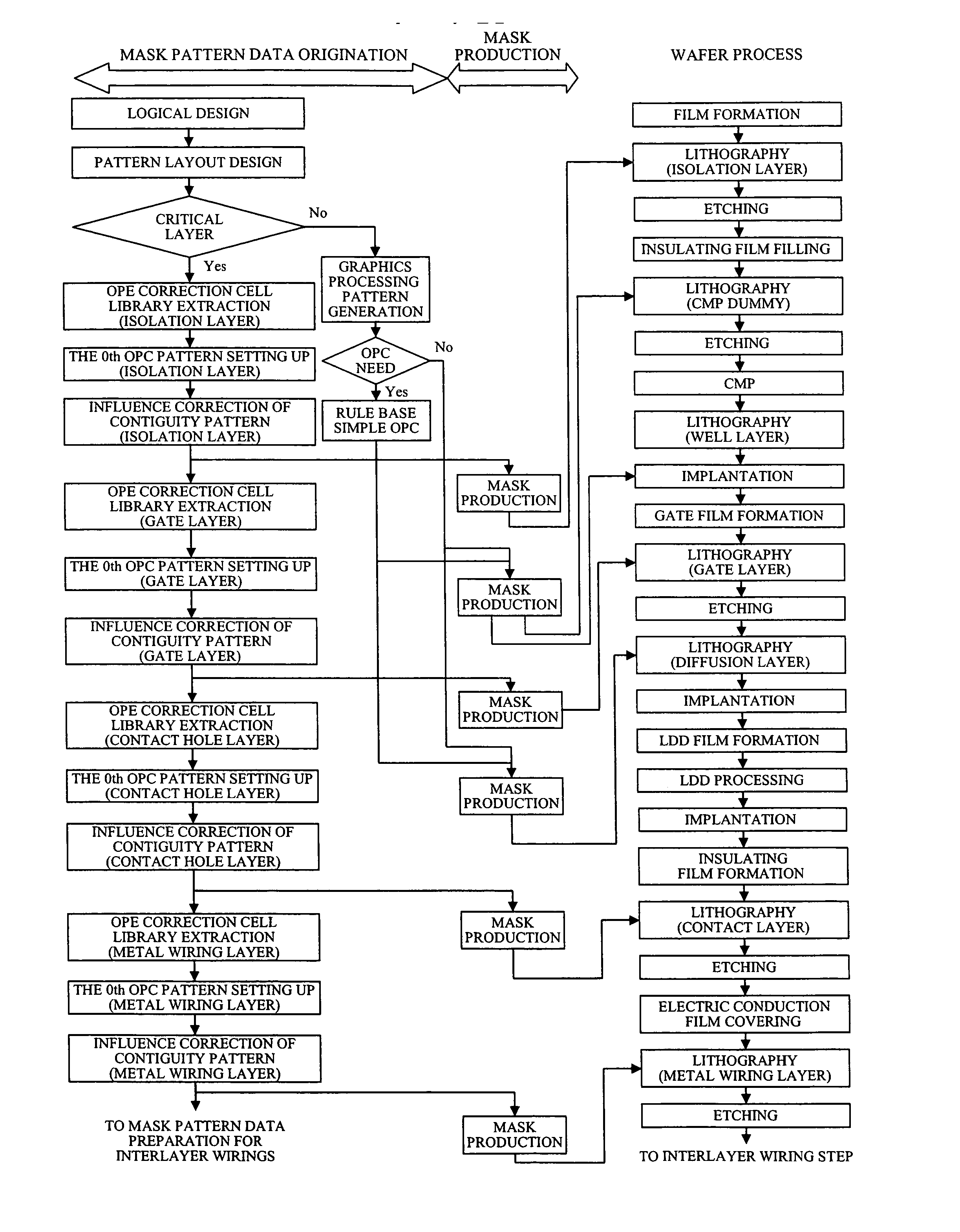
Mask pattern design method and manufacturing method of semiconductor device
a manufacturing method and semiconductor technology, applied in the field of mask pattern design method and manufacturing method of semiconductor devices, can solve the problems of large cost and many storage areas needed for advanced preparations
- Summary
- Abstract
- Description
- Claims
- Application Information
AI Technical Summary
Benefits of technology
Problems solved by technology
Method used
Image

Examples
embodiment 1
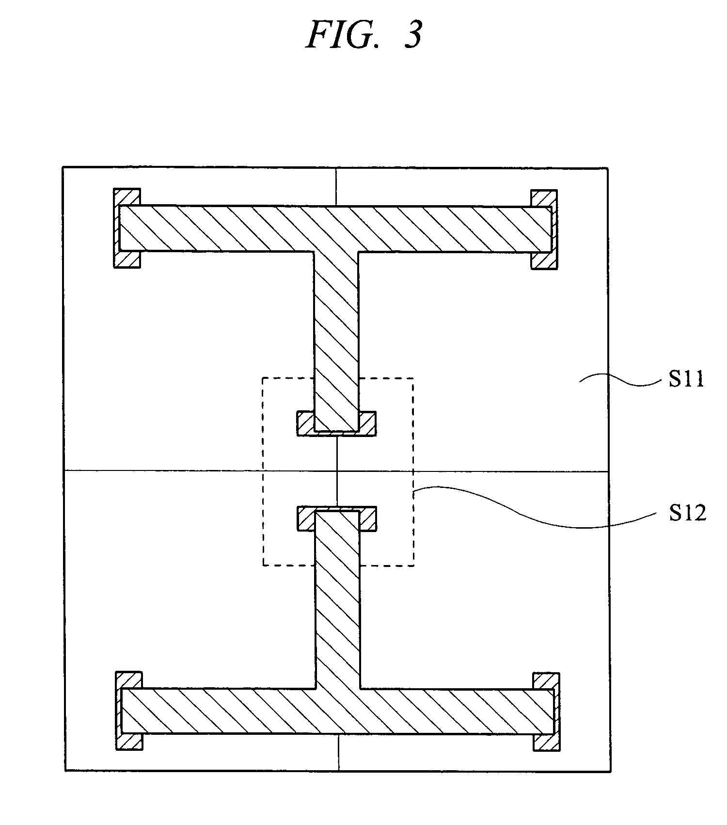
[0092] The mask pattern according to Embodiment 1 of the present invention is designed using a computer etc. In order to verify the validity of the present invention, one of the mask patterns currently used for the gate of SRAM shown in FIG. 3 was used as a cell and the present invention was applied to this. First, the verification experiment of whether to have influence on transfer of a mask pattern according to peripheral environment was conducted. Next, the pattern design technique using genetic algorithm which is the technique of the present invention was applied to the pattern with the strongest influence also in it, and the verification experiment of whether to be able to optimize was conducted. In the experiment described henceforth, verification was performed under lithography conditions as shown in FIG. 48.
[0093] The above-mentioned transfer pattern is generated by optical simulation software. “SOLID-C” (trademark) of Litho Tech Japan Corp. is known as a producer of this s...
verification experiment 1
[Verification Experiment 1]
[0094] First, the verification experiment of whether a mask pattern is influential with the difference in peripheral environment was conducted. The pattern used for verification is shown in FIG. 4. Since these ten patterns are designed by a width of 90 nm, ideal line width is 90 nm. In this experiment, these transfer patterns are created and the influence of peripheral environment is verified by comparing two values, width A (S31), and the length of gap B (S32), shown in FIG. 5 (enlargement of S12 of FIG. 3) as an evaluation value.
[0095] Two evaluation values of the transfer pattern of all the patterns of FIG. 4 are shown in FIG. 49. In P1, since there is no influence of peripheral environment, it has ideal line width, but P2, P3, etc. have the great influence from the circumference, and it turns out that line width S31 and gap S32 are greatly shifted as compared with P1. The transfer patterns of P3 with the greatest influence and ideal pattern P1 are sho...
verification experiment 2
[Verification Experiment 2]
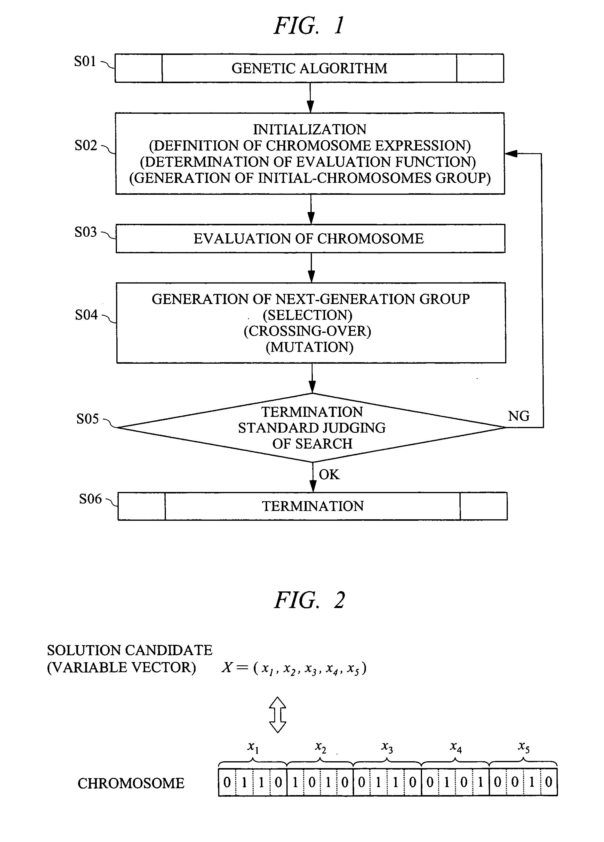
[0096] The verification experiment of whether the influence by peripheral environment proved in verification experiment 1 is solvable with the technique of the present invention was conducted. In this verification experiment 2, the simulation which optimizes P3 (FIG. 7) of the pattern which was the most influential in verification experiment 1 making the mask pattern of P1 (FIG. 8) nearest to an ideal a target was performed as easiest example. In this simulation, it optimized with the technique of the present invention by making into an optimizing parameter 2 places S71 and S72 in the cell shown in FIG. 9 (enlargement of the transfer pattern of S12 of FIG. 3).
[0097] Below, the application method of genetic algorithm is described. Since the calculation procedure of genetic algorithm is as having described in the above “Summary of the Invention”, here is explained the detail of each step.
“Initialization: Definition of Chromosome Expression”
[0098] In this s...
PUM
| Property | Measurement | Unit |
|---|---|---|
| width | aaaaa | aaaaa |
| width | aaaaa | aaaaa |
| thickness | aaaaa | aaaaa |
Abstract
Description
Claims
Application Information