
Semiconductor devices and methods of manufacture thereof

Active Publication Date: 2007-04-05
INFINEON TECH AG
View PDF92 Cites 133 Cited by
  • Summary
  • Abstract
  • Description
  • Claims
  • Application Information

AI Technical Summary

Benefits of technology

[0014] Advantages of preferred embodiments of the present invention include providing novel methods of fabricating transistor devices and structures thereof. Multiple gate CMOS devices may be manufactured, wherein the PMOS transistor and NMOS transistor of the multiple gate CMOS devices have a substantially symmetric Vt. The thickness of the metal gate materials, and / or the dopant level of the gate electrode material, establish the work function of the transistor gate electrodes, and thus establishes the threshold voltage Vt of the transistors. In some embodiments, the same material is preferably used for the gate of the PMOS and NMOS transistor, resulting in reduced efforts that would be required for depositing and etching two different gate materials, and also resulting in the prevention of contamination in manufacturing process tools. In other embodiments, a single type of gate material is deposited, and either the PMOS device or the NMOS transistor gate electrode material is implanted with a dopant species to adjust the work function.

Problems solved by technology

Conventional bulk single-gate planar MOSFET devices cannot achieve the requested performance for future technology nodes of 45 nm or beyond.
However, multiple gate transistors such as FinFETs are more difficult and complicated to manufacture than planar CMOS devices, and they require distinctly different materials and introduce a variety of processing challenges.
However, it is difficult to find materials, device structures, and manufacturing processes that will achieve a symmetric threshold voltage Vt, as devices are made smaller, and particularly for advanced transistor designs having multiple gates.

Method used


Image

  • Semiconductor devices and methods of manufacture thereof
  • Semiconductor devices and methods of manufacture thereof
  • Semiconductor devices and methods of manufacture thereof

Examples


Embodiment Construction

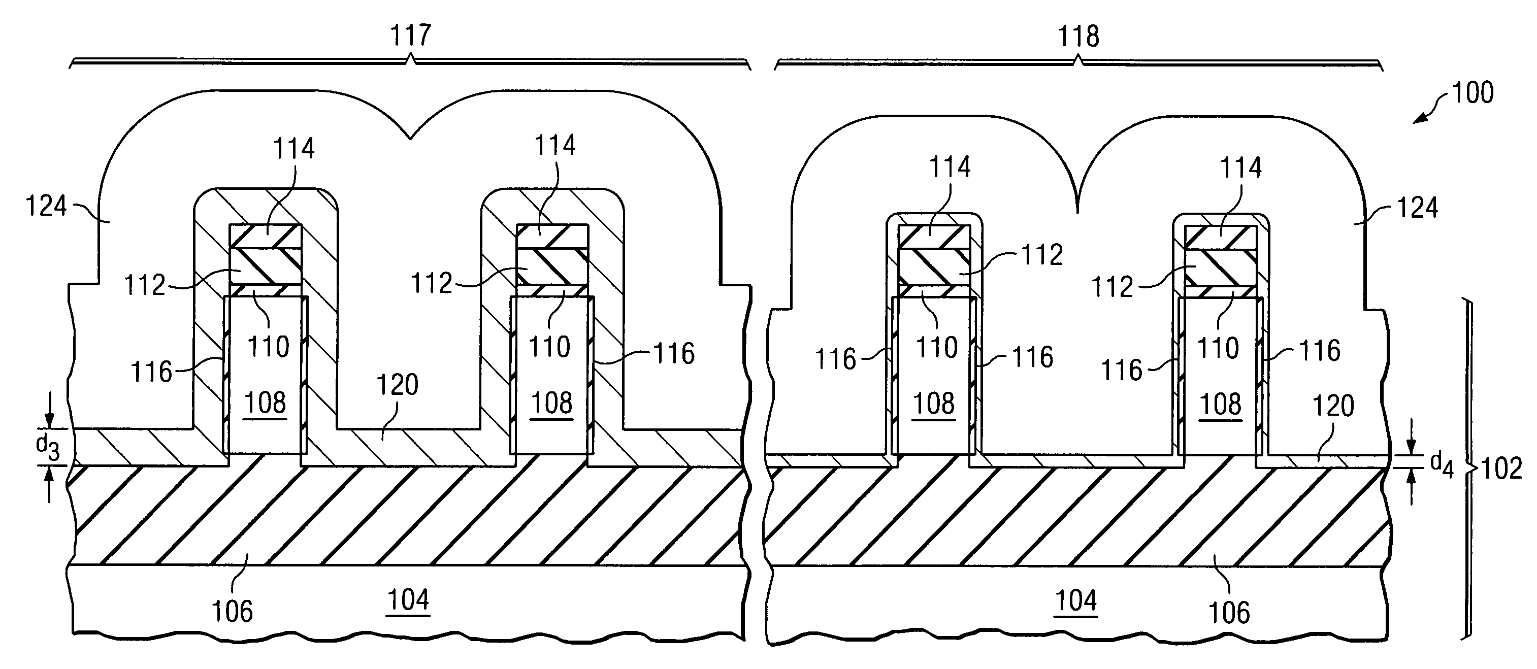
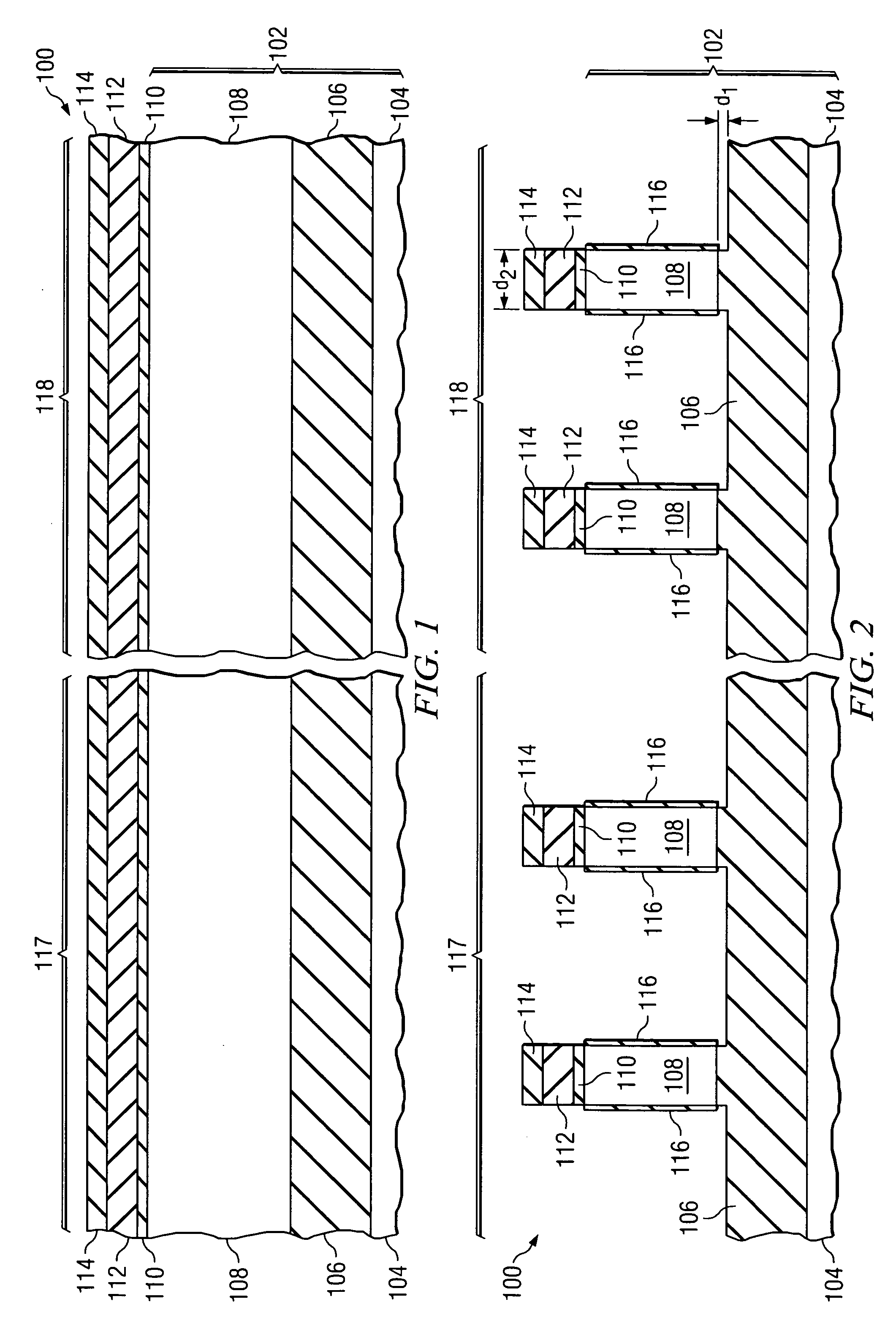
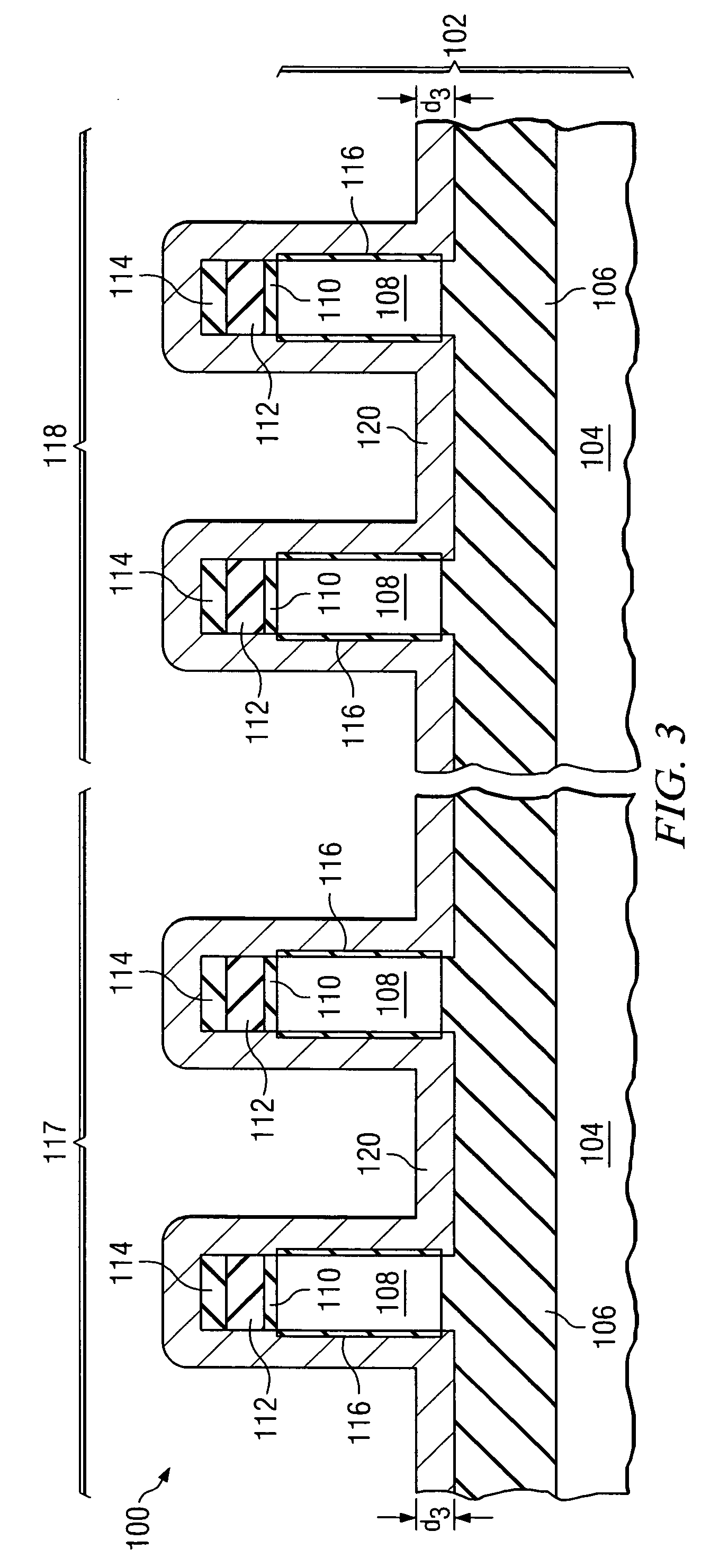
[0030] The making and using of the presently preferred embodiments are discussed in detail below. It should be appreciated, however, that the present invention provides many applicable inventive concepts that can be embodied in a wide variety of specific contexts. The specific embodiments discussed are merely illustrative of specific ways to make and use the invention, and do not limit the scope of the invention.

[0031] In electronics, the “work function” is the energy, usually measured in electron volts, needed to remove an electron from the Fermi level to a point an infinite distance away outside the surface. Work function is a material property of any material, whether the material is a conductor, semiconductor, or dielectric.

[0032] Semiconductor materials have traditionally been used in the past as a gate electrode material for transistor devices. The work function of a semiconductor material can be changed by doping the semiconductor material. For example, undoped polysilicon ...


PUM


Abstract

Semiconductor devices and methods of manufacture thereof are disclosed. A complimentary metal oxide semiconductor (CMOS) device includes a PMOS transistor having at least two first gate electrodes comprising a first parameter, and an NMOS transistor having at least two second gate electrodes comprising a second parameter, wherein the second parameter is different than the first parameter. The first parameter and the second parameter may comprise the thickness or the dopant profile of the gate electrode materials of the PMOS and NMOS transistors. The first and second parameter of the at least two first gate electrodes and the at least two second gate electrodes establish the work function of the PMOS and NMOS transistors, respectively.

Description

TECHNICAL FIELD [0001] The present invention relates generally to semiconductor devices, and more particularly to transistors having multiple gates and methods of manufacture thereof. BACKGROUND [0002] Semiconductor devices are used in a variety of electronic applications, such as personal computers, cell phones, digital cameras, and other electronic equipment, as examples. Semiconductor devices are typically fabricated by sequentially depositing insulating or dielectric layers, conductive layers, and semiconductive layers of material over a semiconductor substrate, and patterning the various layers using lithography to form circuit components and elements thereon. [0003] A transistor is an element that is utilized extensively in semiconductor devices. There may be millions of transistors on a single integrated circuit (IC), for example. A common type of transistor used in semiconductor device fabrication is a metal oxide semiconductor field effect transistor (MOSFET). Conventional ...

Claims


Application Information

Patent Timeline
IPC IPC(8): H01L29/76
CPCH01L21/823821H01L21/823842H01L21/823857H01L21/845H01L27/1211H01L29/785H01L29/66803H01L21/18
Inventor SCHULZ, THOMASLUAN, HONGFA
Owner INFINEON TECH AG
Features
  • Generate Ideas
  • Intellectual Property
  • Life Sciences
  • Materials
  • Tech Scout
  • Unparalleled Data Quality
  • Higher Quality Content
  • 60% Fewer Hallucinations
Learn More