[0008] The present invention was made in consideration of the foregoing problems. A
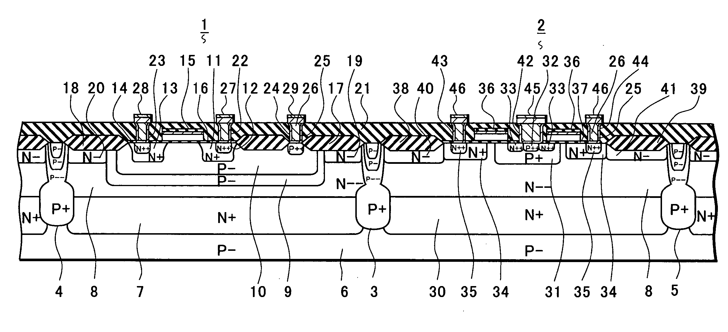
semiconductor device of the present invention includes an isolation region which partition a semiconductor layer into a plurality of element formation regions, a first semiconductor element formed in a first of the element formation regions, and a second semiconductor element formed in a second of the element formation regions, the second element formation region being adjacent to the first element formation region. The semiconductor device includes that a plurality of first
conduction type diffusion
layers are coupled to form the isolation region located between the first and second of the element formation regions, and the first
conduction type diffusion layers are respectively joined to second
conduction type diffusion layers, which respectively constitute the first and second semiconductor elements, to thereby form PN junction regions. Therefore, the semiconductor device of the present invention makes it possible to reduce device size by suppressing extension of diffusion of the first conduction type diffusion layers which constitute the isolation region.
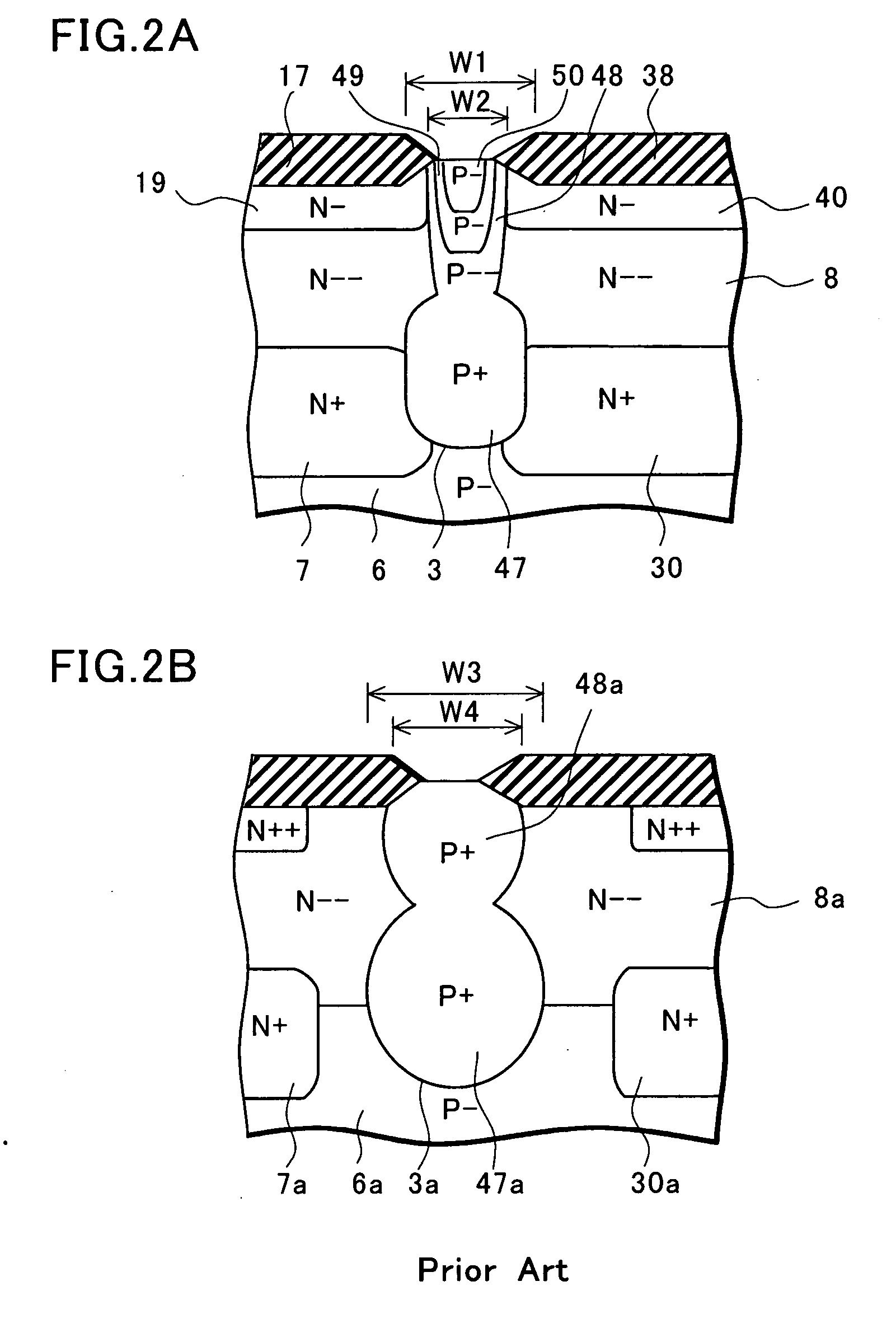
[0009] Moreover, the semiconductor device of the present invention includes that the first conduction type diffusion layers, which constitute the isolation region and which are formed from a surface of the semiconductor layer, are formed by superposing a plurality of diffusion layers having different
impurity concentrations, and a first conduction type diffusion layer having the lowest
impurity concentration forms the PN junction regions. Therefore, the semiconductor device of the present invention makes it possible to improve withstand
voltage characteristics by setting the
impurity concentration in the first conduction type diffusion layer lower in the vicinity of the PN junction region.
[0010] Moreover, the semiconductor device of the present invention includes that the first conduction type diffusion layers formed from the surface of the semiconductor layer are formed by superposing the plurality of diffusion layers in a way that a diffusion layer closer to the center thereof has higher impurity concentrations. Therefore, the semiconductor device of the present invention can reduce resistance of the isolation region, and can prevent inversion of the surface of the isolation region due to a
metal wiring layer, by setting the impurity concentration in the isolation region higher in the vicinity of the surface of the semiconductor layer.
[0011] A method of manufacturing a semiconductor device of the present invention includes the steps of: preparing a first conduction type semiconductor substrate, forming a first conduction type buried diffusion layer for an isolation region, and second conduction type buried diffusion layers for semiconductor elements, in the substrate, forming a second conduction type epitaxial layer on the substrate, and thereafter forming first conduction type diffusion layers for the isolation region and second conduction type diffusion layers for the semiconductor elements, from a surface of the epitaxial layer. In the method: the first and second conduction type buried diffusion layers are joined to form a PN junction region, whereby the second conduction type buried diffusion layers suppress widthwise diffusion of the first conduction type buried diffusion layer, and the first and second conduction type diffusion layers are joined to form the PN junction region, whereby the second conduction type diffusion layers suppress widthwise diffusion of the first conduction type diffusion layer. Therefore, in the present invention, the second conduction type buried diffusion layer and the second conduction type diffusion layer suppress widthwise diffusion of the first conduction type buried diffusion layer and the first conduction type diffusion layer which constitute the isolation region. Thus, the present invention makes it possible to reduce the device size by suppressing extension of diffusion of the isolation region.
[0012] Moreover, the method of manufacturing a semiconductor device of the present invention includes that the first conduction type diffusion layers are formed by superposing a plurality of diffusion layers having different impurity concentrations, and a first conduction type diffusion layer having the lowest impurity concentration is formed with the greatest width and is joined to the second conduction type diffusion layers to form the PN junction region. Therefore, in the present invention, the diffusion layer having the lowest impurity concentration is located on the outermost periphery of the first conduction type diffusion layer. Thus, the present invention makes it possible to improve the withstand
voltage characteristics by reducing the impurity concentration in the first conduction type diffusion layer in the vicinity of the PN junction region.

