
Organic light emitting devices having latent activated layers

a technology of activated layer and organic light, which is applied in the direction of liquid/solution decomposition chemical coating, discharge tube luminescnet screen, natural mineral layered products, etc. it can solve the problems of vapor deposition not desirable for continuous manufacture using air sensitive precursors, and the reaction of known electron donors with air or moistur

Inactive Publication Date: 2007-04-05
GENERAL ELECTRIC CO
View PDF10 Cites 16 Cited by
  • Summary
  • Abstract
  • Description
  • Claims
  • Application Information

AI Technical Summary

Benefits of technology

[0204] The previously described embodiments of the present invention have many advantages, including, providing OLED devices with greater conductivity leading to possible increases in OLED light emitting efficiencies.

Problems solved by technology

The reactive nature of these materials can cause problem when forming multi-layer devices.
Furthermore, known electron donors typically react with air or moisture and may decompose during manufacture.
Vapor deposition is not desirable for continuous manufacture.
Vapor deposition is not desirable for continuous manufacture using air sensitive precursors.

Method used


Image

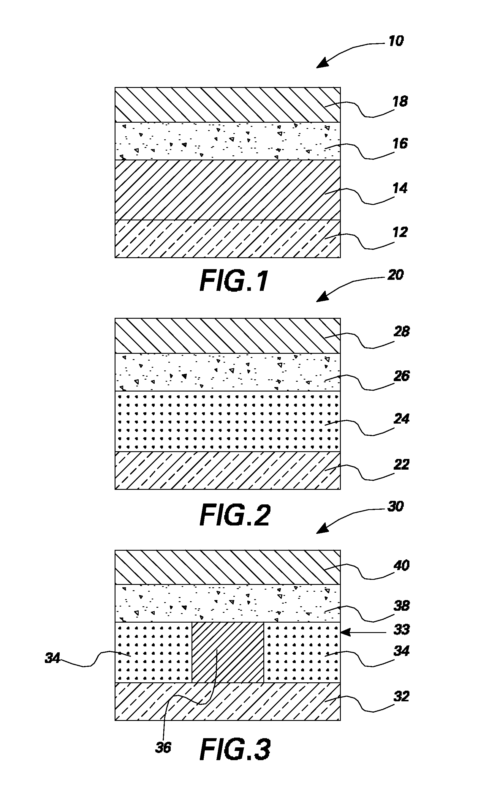
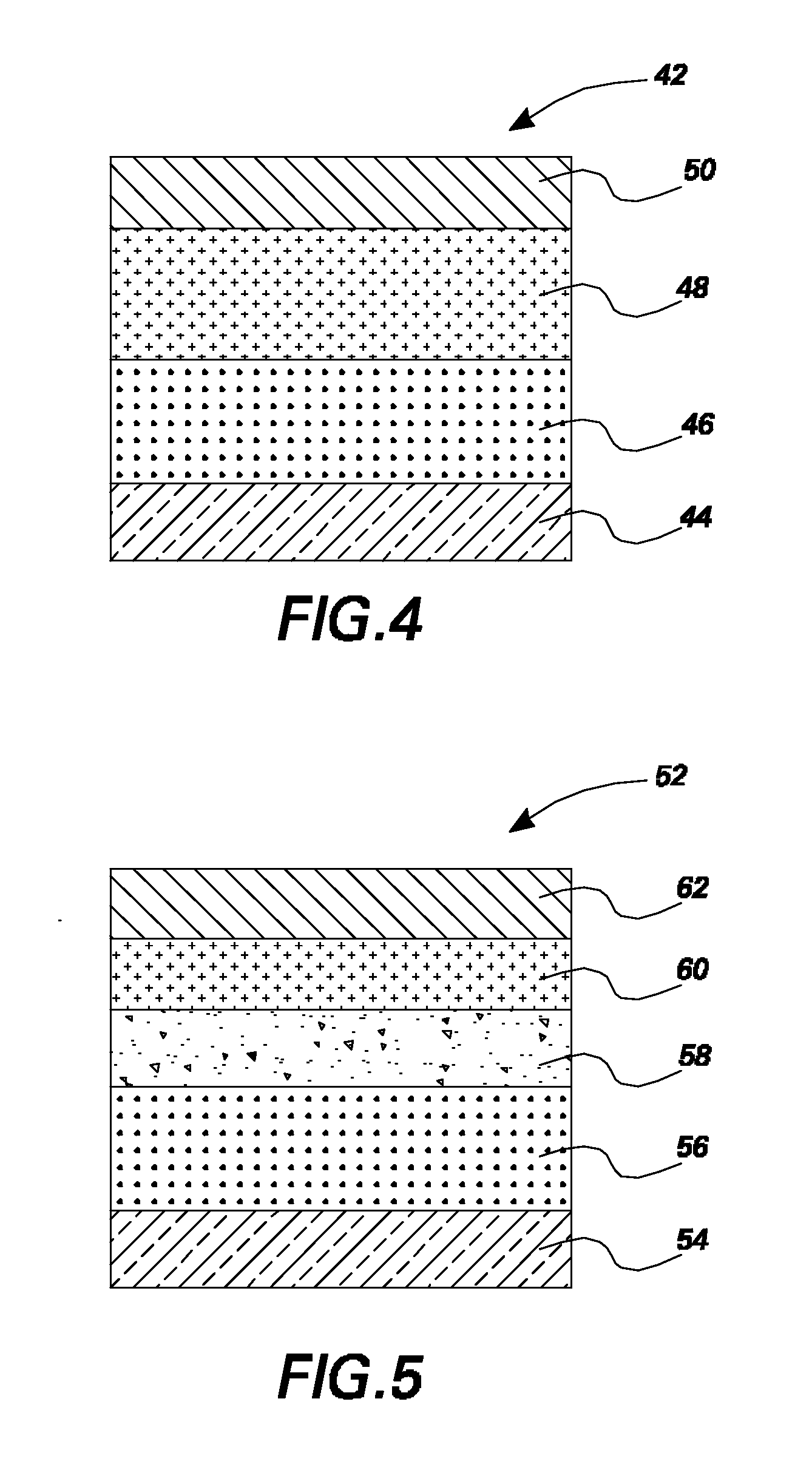
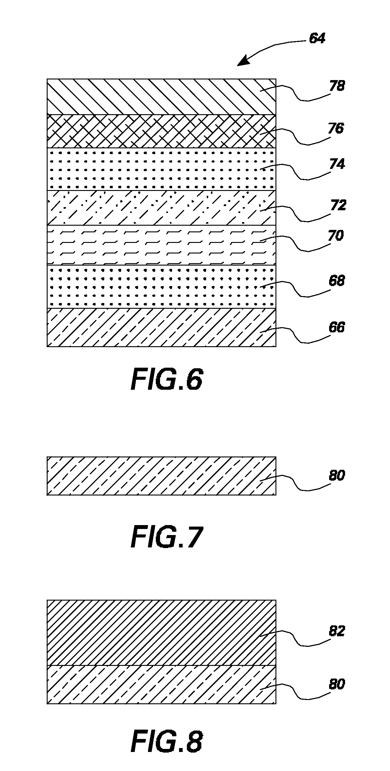
  • Organic light emitting devices having latent activated layers
  • Organic light emitting devices having latent activated layers
  • Organic light emitting devices having latent activated layers

Examples


example 2

[0179] devices were fabricated. The OLEDs consisted of a blue light-emitting polymer (LEP), ADS329BE [poly(9,9-dioctylfluoenyl-2,7-diyl)—end capped with N,N-Bis(4-methylphenyl)-aniline], obtained from American Dye Sources, Inc, Canada, and used as received without any further purification, as the emissive layer material.

[0180] s were fabricated as follows. ITO coated glass, patterned using standard photolithography techniques, was used as the anode substrate. The OLEDs employ an ITO anode with and without an additional anode-activation layer but otherwise the same structure. As shown in the Table 2, both device A and device B had the same ITO anode except that the ITO substrate in device B was further UV-ozoned for 5 minutes prior to the application of ADS329BE. Devices C and D had the same anode-activation layer of PEDOT-TMA (about 40 to 45 nanometer) except that the PEDOT-TMA layer in the device D was further UV-ozoned for about 5 minutes prior to the application of ADS329BE. Bot...

example 3

[0183] A 2 liter, 3-neck flask was charged with Adogen 464 (about 23 grams), 2-bromo-propane (about 235 milliliter), potassium hydroxide (saturated, aq, about 1.2 liter), and freshly cracked and distilled cyclopentadiene (41 milliliter). The contents were stirred with a mechanical stirrer and heated to about 80° C. for 24 hours. Gas chromatography analysis of the top layer showed excellent conversion to tetra-iso-propylcyclopentadiene. The entire reaction mixture was poured into a separatory funnel. Addition of water and hexanes broke up the emulsion and the top layer was collected. The bottom aqueous layer was washed with hexanes, and a total of about 1.5 liter of organic solvents was collected. The organic layer was then dried with magnesium sulfate and then filtered and washed with more hexanes. The total organics were then subjected to rotary evaporation (30 mmHg) and 80° C. to remove hexanes and leave a higher boiling oil. The oil was then subjected to vacuum distillation throu...

example 4

[0189] Four OLED devices were fabricated. Two solutions were prepared in the same glovebox (moisture and oxygen was less than 1 ppm and 3 ppm, respectively) prior to device fabrication. The first solution (referred to OAP9903:SR454) included a green light-emitting polymer poly[(9,9-dioctylfluoren-2,7-diyl)-alt-co-(benzo[2,1,3]thiadiazol-4,7-diyl)] (OPA9903) obtained from H. W. Sands, Corporation, Jupiter, Fla. 33477, USA and an acrylate-based adhesive ethoxylated (3) trimethylolpropane triacrylate (SR454) obtained from Sartomer, Exton, Pa. 19341, USA. Both materials were used as received without any further purification. The mixture solution was prepared by mixing about 2.5 milliliter of a 2% OPA9903 solution in p-xylene with about 2 milliliter of a 1% SR454 solution in p-xylene. The resulting ratio of SR454 to OPA9903 was about 30 wt %. The second solution (referred to as OPA9903:Ba-TPCP) including OPA9903 and Ba-TPCP was prepared by mixing about 1.5 milliliter of a 0.6 wt % OPA990...


PUM

PropertyMeasurementUnit
Work functionaaaaaaaaaa
Temperatureaaaaaaaaaa

Abstract

An organic light emitting device with a latent activator material is presented. An organic light emitting device including activation products of a latent activator material is also presented. Embodiments of patterned organic light emitting devices are also contemplated wherein patterning can occur prior or post fabrication of the devices. A method of fabricating an organic light emitting device with a latent activator material or with activation products of an activator material is also provided.

Description

CROSS REFERENCE TO RELATED APPLICATIONS [0001] This application is a continuation in part of copending application, Ser. No. 11 / 243194, filed Oct. 4, 2005, the entire contents of which is incorporated by reference herein.STATEMENT REGARDING FEDERALLY SPONSORED RESEARCH & DEVELOPMENT [0002] This invention was made with Government support under contract number 70NANB3H3030 awarded by National Institute of Standards and Technology. The Government has certain rights in the invention.BACKGROUND [0003] The invention relates generally to organic electronic devices. The invention in particular relates to organic light emitting devices. [0004] Organic electronic devices include organic light emitting devices and organic photovoltaic devices. Organic electronic devices operate by injection of charges, which combine to result in radiation of energy as in a light emitting device, or separation of charges as in a photovoltaic device. As will be appreciated by one skilled in the art, an organic l...

Claims


Application Information

Patent Timeline
IPC IPC(8): H01L51/52H01L51/56
CPCC23C18/08C23C18/14H01L51/5221H01L51/5052H01L51/0021Y10T428/31678C23C18/143C23C18/145H10K71/60H10K50/155H10K50/165H10K50/82
Inventor LEWIS, LARRY NEILHUANG, QINGLANFOUST, DONALD FRANKLIN
Owner GENERAL ELECTRIC CO
Learn More