Ferrite substrate for thin-film inductors, thin-film common mode filter using the substrate, thin-film common mode filter array using the substrate and manufacturing method of the substrate

Inactive Publication Date: 2007-04-05
TDK CORPARATION
View PDF1 Cites 2 Cited by
  • Summary
  • Abstract
  • Description
  • Claims
  • Application Information

AI Technical Summary

Benefits of technology

[0011] It is therefore an object of the present invention to provide a ferrite substrate for thin-film inductors, with a higher surface insulation resistance and less surface-degradation, a thin-film common mode filter using the substrate, a thin-film common mode filter array using the substrate, and a manufacturing method of the substrate.
[0013] A further object of the present invention is to provide a ferrite substrate for thin-film inductors, on a surface of which terminals can be precisely formed without difficulty, a thin-film common mode filter using the substrate, a thin-film common mode filter array using the substrate, and a manufacturing method of the substrate.
[0016] By being given the crystalline structure densified by HIP with the above-mentioned ferrite composition, the substrate achieves high surface insulation resistance of 2×10¹⁰ Ω·cm or more, and the common mode filter produced from the substrate can acquire enough electrical isolation between the coils. And, there is no change (degradation) in bulk insulation resistance and surface insulation resistance of the substrate after being annealed in the thin film process. Further, mechanical strength (bending strength) of the substrate is enhanced to the value at least 1.5 times larger than that of substrate produced by conventional hot forming press method, which is a enough strength for the substrate to undergo the thin film process. Furthermore, the densified substrate-surface with almost no voids can prevent electrical trouble due to plating on unwanted portion when the terminals and the like are formed by plating. In addition, the terminal patterns are able to being formed precisely because of the densified substrate-surface.
[0020] By undergoing HIP, after being set into the above-mentioned ferrite composition and sintered, the obtained substrate achieves a high surface insulation resistance value of 2×10¹⁰ Ω·cm or more, and the common mode filter produced from the substrate can acquire enough electrical isolation between the coils. Further, there is no change or degradation in bulk insulation resistance and surface insulation resistance of the substrate after being annealed in the thin film process. Further, mechanical strength or bending strength of the substrate is enhanced to the value at least 1.5 times larger than that of substrate produced by conventional hot forming press method, which is a enough strength for the substrate to undergo the thin film process. Furthermore, the densified substrate-surface with almost no voids can prevent electrical trouble due to plating on unwanted portion when the terminals and like are formed by plating. In addition, the terminal patterns are able to being formed precisely because of the densified substrate-surface.

Problems solved by technology

Conventional ferrite substrate for the thin-film common mode filter, however, has a porous crystalline structure with voids and such on its surface, which causes low insulation resistance on its surface and large surface-degradation.
The ferrite substrate, therefore, has too poor mechanical strength to undergo thin-film process, and moreover, it has been difficult to form precisely the terminals on the substrate surface.

Method used


Image

  • Ferrite substrate for thin-film inductors, thin-film common mode filter using the substrate, thin-film common mode filter array using the substrate and manufacturing method of the substrate
  • Ferrite substrate for thin-film inductors, thin-film common mode filter using the substrate, thin-film common mode filter array using the substrate and manufacturing method of the substrate
  • Ferrite substrate for thin-film inductors, thin-film common mode filter using the substrate, thin-film common mode filter array using the substrate and manufacturing method of the substrate

Examples


Embodiment Construction

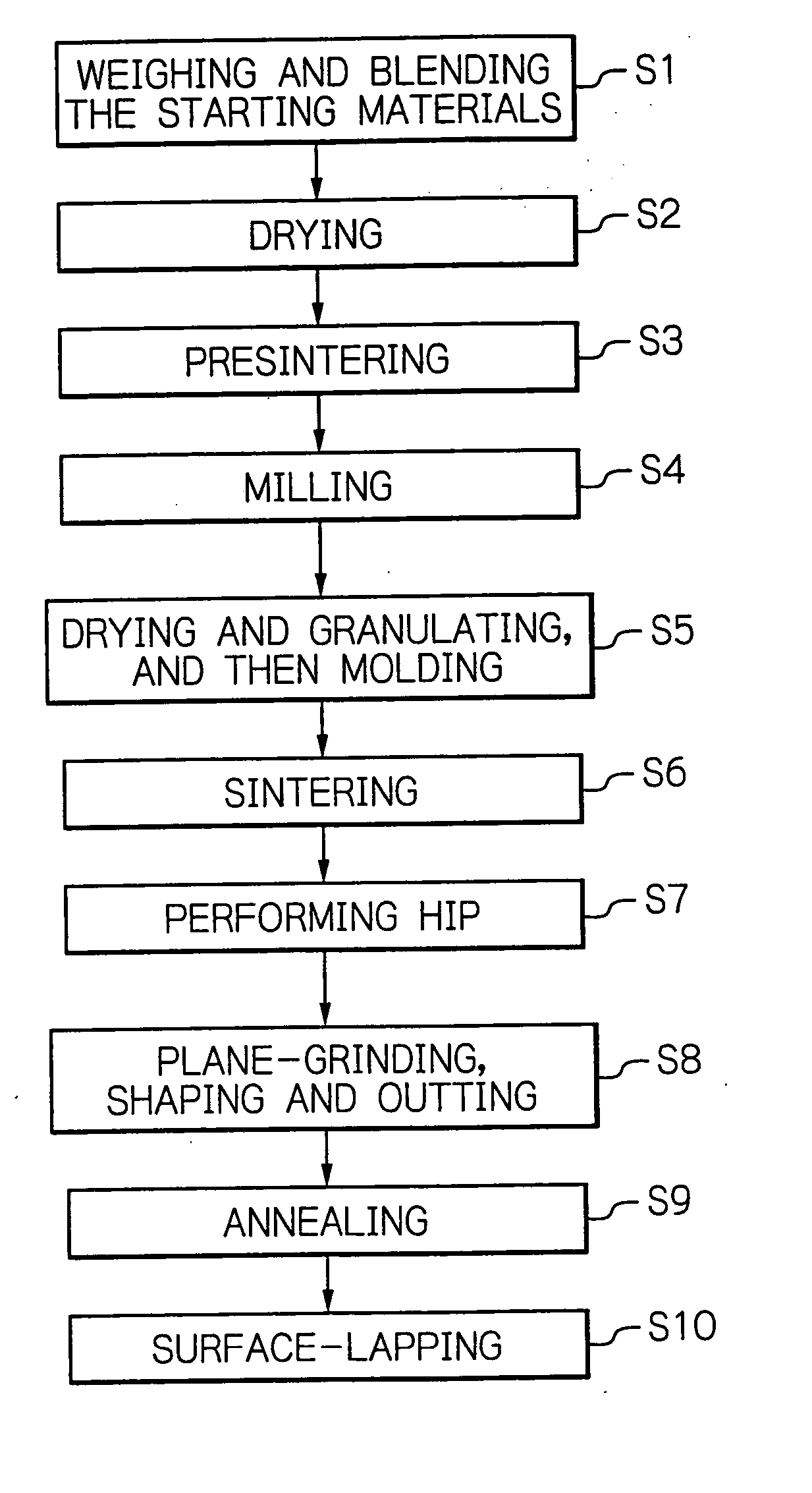
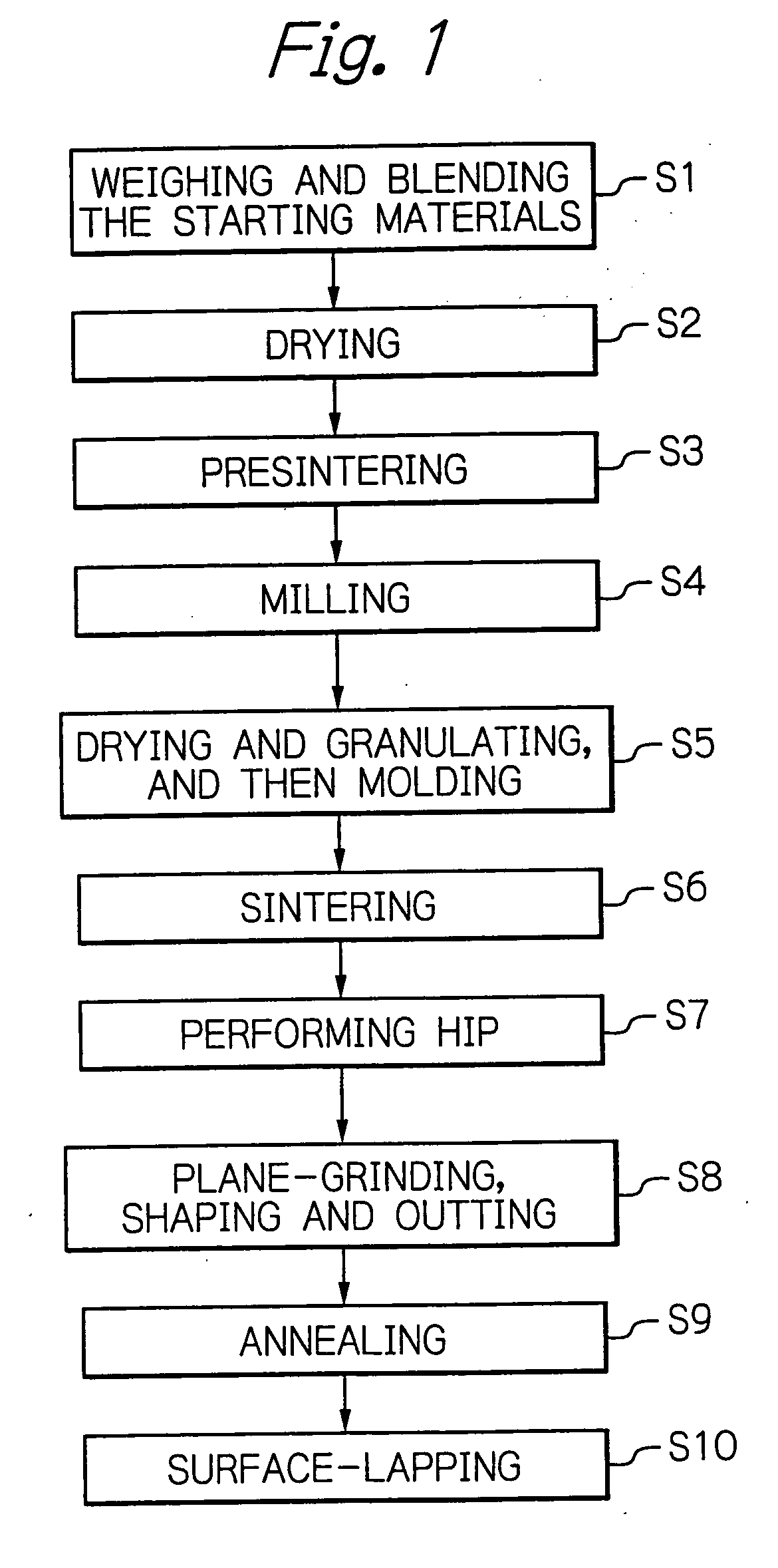
[0050]FIG. 1 schematically illustrates some steps in a preferred embodiment of a manufacturing method of a ferrite substrate for thin-film inductors according to the present invention. The manufacturing steps of the ferrite substrate will be described in detail with reference to the figure hereafter.

First example of the substrate composition

[0051] First, raw materials are weighed according to the blend table so that obtained ferrite substrates will have a predetermined composition, and then are blended by adding purified water (step S1). The predetermined composition is Fe2O3: 40 to 55 mol %, NiO: 15 to 30 mol %, and ZnO: 20 to 40 mol %.

[0052] Next, the obtained blended slurry is dried (step S2), and presintered (step S3).

[0053] Then, the obtained presintered material is milled with purified water (step S4). The milling is accompanied by adding 150 to 750 ppm in Bi2O3. CaCO3 and such also may be added.

[0054] Next, the obtained milled material is dried and granulated, and then ...


PUM

PropertyMeasurementUnit
Diameteraaaaaaaaaa

Abstract

A ferrite substrate for thin-film inductors is provided by means of blending raw materials to meet a composition of di-iron trioxide (Fe2O3): 40 to 55 molt %, nickel oxide (NiO): 5 to 35 molt, zinc oxide (ZnO): 10 to 40 molt %, and bismuth trioxide (Bi2O3): 150 to 750 ppm, or of Fe2O3: 40 to 55 molt %, NiO: 5 to 35 mol %, ZnO: 10 to 40 mol %, cupric oxide (CuO): 5 to 10 molt, and manganese dioxide (MnO2): 0.5 to 2 molt %, and then molding and sintering the blended material, and applying hot isostatic pressing to the sintered article. A thin-film common mode filter and a thin-film common mode filter array using the ferrite substrate and the manufacturing method of the substrate are also provided.

Description

CROSS REFERENCE TO RELATED APPLICATION [0001] This application is a divisional application of Application Ser. No. 10 / 862,533, filed Jun. 8, 2004.PRIORITY CLAIM [0002] This application claims priority from Japanese patent application No.2003-163563, filed on Jun. 9, 2003, which is incorporated herein by reference. BACKGROUND OF THE INVENTION [0003] 1. Field of the Invention [0004] The present invention relates to a ferrite substrate for thin-film inductors, to a thin-film common mode filter using the substrate, to a thin-film common mode filter array using the substrate, and to a manufacturing method of the substrate. [0005] 2. Description of the Related Art [0006] Common mode filter is a device for suppressing common mode currents that cause electromagnetic interference in parallel transmission lines. The common mode filter has magnetically coupled inductors to remove in-phase noise component. [0007] Thin-film common mode filter miniaturized and highly integrated by forming bilayer...

Claims


Application Information

Patent Timeline
IPC IPC(8): H01F1/00C04B35/26C04B35/30C04B35/645H01F1/34H01F17/04H01F27/00H01F41/02
CPCC04B35/265C04B35/6262C04B35/64C04B35/645C04B35/6455C04B2235/3208C04B2235/3267C04B2235/3279C04B2235/3281C04B2235/3284C04B2235/3298C04B2235/662C04B2235/77C04B2235/96C04B2235/9607C04B2235/963H01F1/344H01F41/0246
Inventor SHOJI, SHIGERUSATO, AKIRAKAWAGUCHI, YUKIOTANAKA, KAZUMITSUTANISHIMA, TOSHIKAZU
Owner TDK CORPARATION
Why Eureka
Try Eureka