Laser resist transfer for microfabrication of electronic devices

a technology of electronic devices and laser resists, applied in the direction of diffusion transfer processes, instruments, circuit masks, etc., can solve the problems of difficulty and cost of combining steps (i)-v) in any type of automated, continuous fabrication system or apparatus, and the requirement for careful control of ambient illumination

Inactive Publication Date: 2007-04-05
EASTMAN KODAK CO
View PDF17 Cites 42 Cited by
  • Summary
  • Abstract
  • Description
  • Claims
  • Application Information

AI Technical Summary

Benefits of technology

[0032] The invention and its objects and advantages will become more apparent in the detailed description of the preferred embodiment presented below.

Problems solved by technology

Because of the very different nature of processes carried out in each of these steps, it would be difficult and costly to combine steps (i)-(v) in any type of automated, continuous fabrication system or apparatus.
Among disadvantages of conventional photoresist use is the requirement for careful control of ambient illumination until curing is complete.
However, in spite of these advantages, some performance drawbacks remain.
Adhesive transfer, used in the methods of each of these disclosures, has inherent limitations for maintaining precise tolerances.
FIG. 2 shows a familiar problem with adhesive transfer.
This problem occurs as donor sheet 70 is pulled away from substrate 18.
One of two problems is possible, however, as illustrated in FIG. 2.
A second possible problem relates to a portion of the adhered resist transfer layer 68 that is not perfectly affixed to substrate 18, due to some slight surface imperfection for example, or due to excessive thickness or strength of the surrounding un-adhered resist donor on resist transfer layer 68.
However, in some cases, this effect could cause jagged edges of surface features where excessive resist material has been removed.
But because it is not possible to obtain perfect separation between adhered and un-adhered portions of a pattern, adhesive transfer, as proposed in the Burberry et al.
'384, and Toyoda '74705 disclosures, suffers from inherent problems in maintaining precision edge definition.
This, in turn, limits the dimensional resolution that can be obtained for a resist pattern formed using adhesion bonding methods.
A further, significant disadvantage of adhesive transfer relates to overall energy level requirements.
When a donor sheet is in flush contact with a receiver substrate, the laser spot necessarily loses some amount of heat through thermal diffusion.
Thermal diffusion can be particularly troublesome when the receiving substrate is a metal surface with a high thermal conductivity.
Yet other disadvantages of adhesive transfer relate to the need for intimate, planar surface contact between donor and receiver substrate.
The presence of any type of surface features on the receiver surface tends to separate the donor from the receiver surface, resulting in less-than-ideal bonding conditions for precision transfer using adhesive transfer techniques.
Similarly, dust or dirt particles, inevitable even in controlled “clean room” environments, may settle between the surfaces of the donor and receiver substrate.
Imperfect adhesion bonding caused by dust or other particulate can have a pronounced effect, resulting in a drop-out near the point of contact.

Method used


Image

  • Laser resist transfer for microfabrication of electronic devices
  • Laser resist transfer for microfabrication of electronic devices
  • Laser resist transfer for microfabrication of electronic devices

Examples


example 1

[0068] A donor element comprising a 102 microns polyethylene teraphthalate support containing a subbing layer of 0.43 g / m2 gelatin hardened with dihydroxydioxane was subsequently coated with a transfer assist layer containing (0.332 g / m2) polycyanoacrylate, (0.054 g / m2) IR dye 1, with the following structure:

from a mixture of cyclopentanone, N-methylpyrollidone, and methanol with 0.01 wt % surfactant Silwet L7001 (GE Silicones). This assembly was then overcoated with the resist transfer layer comprising (1.08 g / m2) Foral 85 (hydrogenated rosin ester, Hercules Corp.) binder, (1.08 g / m2) Organic Pigment T-11 from DayGlo Corporation (solid dye solution in a Thermoset Resin Bead of 4-5 micron diameter), (0.118 g / m2) polyvinyl butyral, (0.027 g / m2) Rhodamine 6G dye, and DC1248 (Dow Corning), a silicone surfactant at 0.02 wt % of the solution, from a mixture of methyl ethyl ketone and ethyl alcohol.

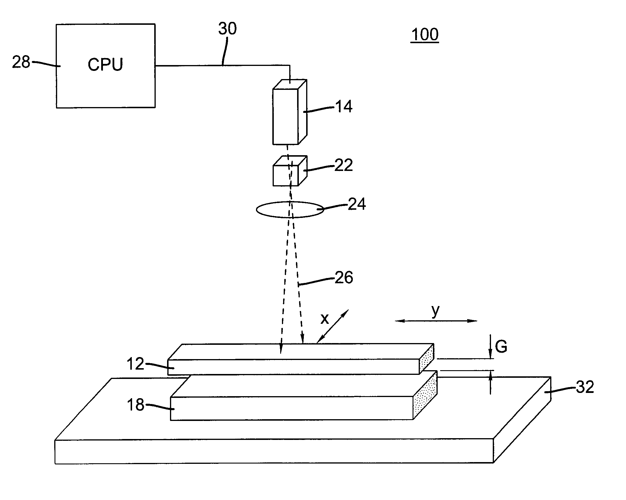
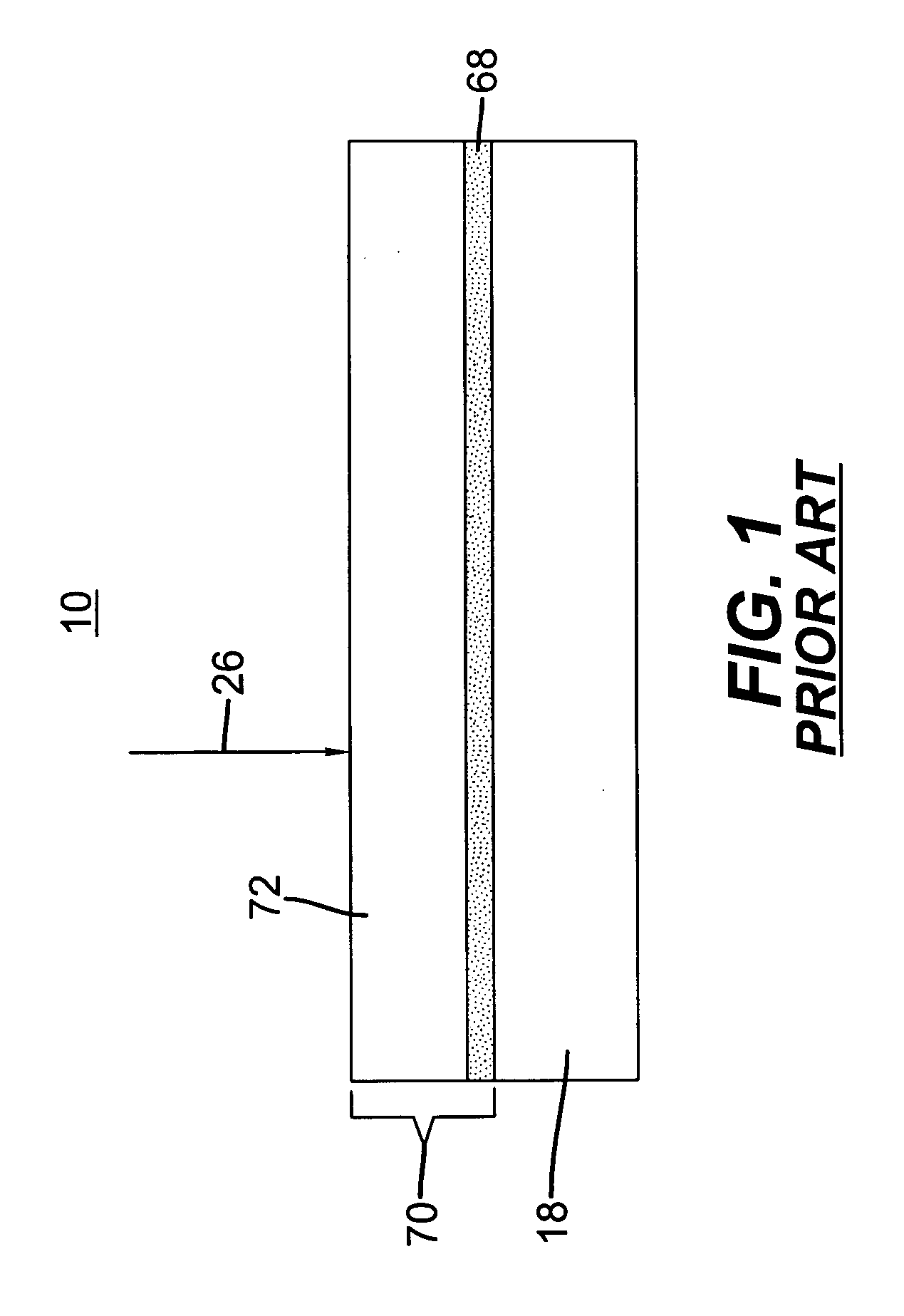
[0069] Donor element 12 was placed on substrate 18, which was composed of a glass plate...
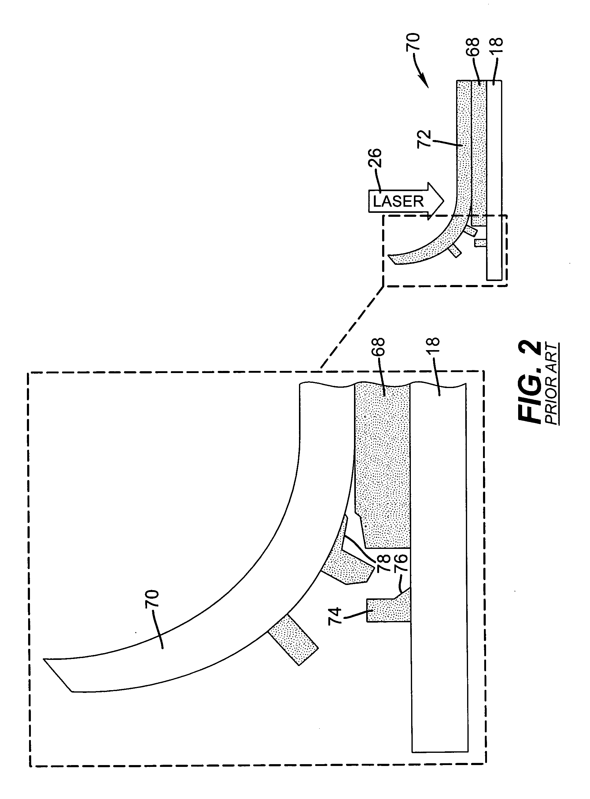
example 2

[0071] For this two-pass example, the steps of Example 1 were completed in a first pass. Then, as the second pass, a second resist material was applied, this time where no spacer particles or beads were used between donor element 12 and substrate 18. This is permissible since existing structures formed in the first pass provide the needed gap G (FIG. 4). That is, for the second pass, existing surface features 74 that were formed during the first pass effectively act as spacers, eliminating the need for spacers 88 as were shown in FIG. 4. Donor element 12 for the second pass used a 4 mil PET support, coated with a first subbing layer of tetrabutoxy titanate (Tyzor TBT, Dupont) coated from a mixture of n-butanol and n-propyl acetate, and a second transfer layer of 0.16 g / m2 cellulose acetate propionate, 0.054 g / m2 IR-2, 0.077 g / m2 Cyan Dye 1, with structure:

0.075 Magenta Dye 1, with structure:

0.069 g / m2 Yellow Dye 1, with structure:

coated from a mixture of MIBK (40%), n-propy...

example 3

[0073] This example followed the same process steps as those described for Examples 1 or 2, with minor exceptions, as follows: [0074] (i) the coated material on the glass substrate is poly silicon; and [0075] (ii) the etch gas atmosphere is sulfur hexafluoride.


PUM

PropertyMeasurementUnit
thickaaaaaaaaaa
diameteraaaaaaaaaa
diameteraaaaaaaaaa

Abstract

A method for forming a resist pattern on a substrate (18) places a donor element (12) having a layer of thermoresist material proximate the substrate. A gap is maintained such that the surface of the layer of thermoresist material is spaced apart from the surface of the substrate by a number of spacing elements. Thermal energy is directed toward the donor element (12) according to the resist pattern, whereby a portion of thermoresist material is transferred from the donor element (12) across the gap by ablative transfer and is deposited onto the substrate (18) forming the resist pattern.

Description

CROSS REFERENCE TO RELATED APPLICATIONS [0001] Reference is made to commonly-assigned copending U.S. patent application Ser. No. ______ (Attorney Docket No. 89243 / RLO), filed herewith, entitled PATTERNING OLED DEVICE ELECTRODES AND OPTICAL MATERIAL by Newman et al.; and U.S. patent application Ser. No. 10 / 944,586, filed Sep. 17, 2004, entitled METHOD OF FORMING A STRUCTURED SURFACE USING ABLATABLE RADIATION SENSITIVE MATERIAL, by Ali et al., the disclosures of which are incorporated herein. FIELD OF THE INVENTION [0002] The present invention relates, in general, to fabrication of microelectronic devices and in particular to fabrication of microelectronic devices using a dry process with a resist formed by laser transfer. BACKGROUND OF THE INVENTION [0003] Lithographic patterning techniques have been employed in conventional fabrication of microelectronic devices, including thin film transistor (TFT) arrays for flat panel application. Conventional photoresist lithographic techniques ...

Claims


Application Information

Patent Timeline
Patent Type & Authority Applications(United States)
IPC IPC(8): G03C8/00
CPCB41M5/38207B41M5/398H05K3/0079H05K2203/0528H05K2203/107B41M2205/08G03F7/26G03F7/38H05K3/06G03F7/34
Inventor TREDWELL, TIMOTHY J.TUTT, LEE W.KAY, DAVID B.HONG, YONGTAEKPEARCE, GLENN T.PHILLIPS, SCOTT E.
Owner EASTMAN KODAK CO
Why Eureka
Try Eureka