Light-emitting device and manufacturing method thereof

Active Publication Date: 2007-04-05
SUZHOU LEKIN SEMICON CO LTD
View PDF7 Cites 10 Cited by
  • Summary
  • Abstract
  • Description
  • Claims
  • Application Information

AI Technical Summary

Benefits of technology

[0020] The present invention provides a light-emitting device and a manufacturing method thereof, capable of preventing a short-circuit between electrodes and improving a light-emission efficiency, brightness and reliability of the light-emitting device.
[0025] According to the present invention, a damage that can be caused on an already grown epitaxial layer can be reduced, and an area of an active layer is increased, so that a light-emission efficiency increases.

Problems solved by technology

However, since the sapphire substrate in an insulator, a rear side contact is impossible during a device fabrication, so that there are lots of difficulties during a manufacturing process.
When a chip size is reduced, an interval between a p-type electrode and an n-type electrode narrows, there is a high possibility that a short-circuit between the electrodes occurs.
Also, there is a problem that a grown epitaxial layer is damaged during drying etching, and generates a defect, resulting in reduction of a light-emission efficiency.
Consequently, these problems reduce brightness and reliability of a light-emitting device.

Method used


Image

  • Light-emitting device and manufacturing method thereof
  • Light-emitting device and manufacturing method thereof
  • Light-emitting device and manufacturing method thereof

Examples


Embodiment Construction

[0030] Reference will now be made in detail to the preferred embodiments of the present invention, examples of which are illustrated in the accompanying drawings.

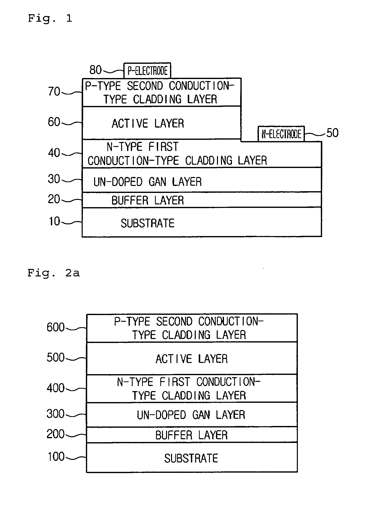
[0031]FIGS. 2A to 2E are cross-sectional views sequentially explaining a process for manufacturing a light-emitting device according to the present invention.

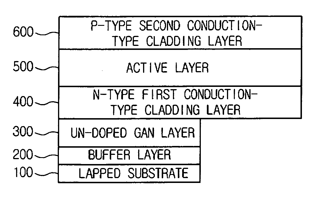
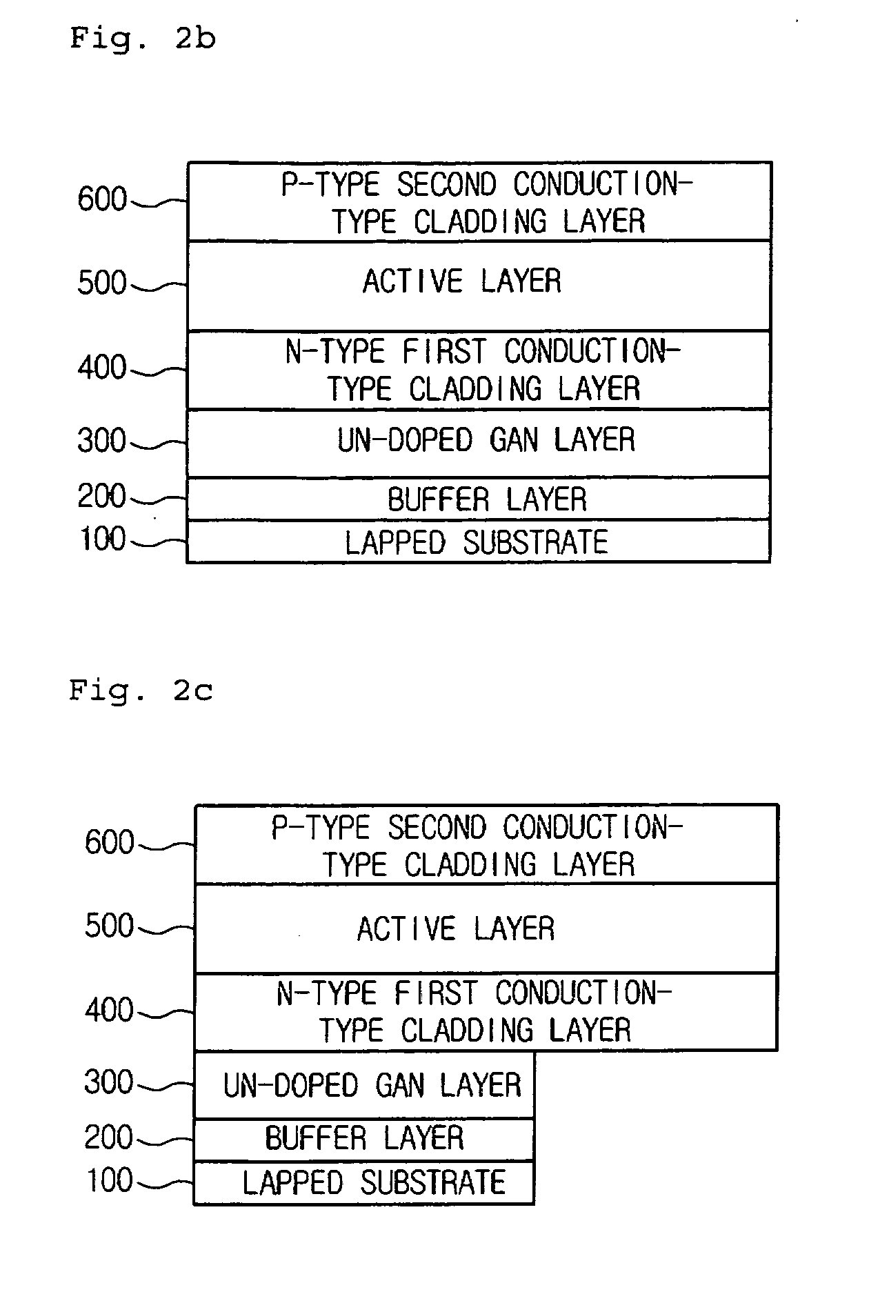
[0032] First, in embodiments of the present invention, a nitride semiconductor using a compound such as GaN, AlN, and InN belonging to a group III and a group V can be independently used or used in combination for the light-emitting device. For example, referring to FIG. 2A, a light-emitting device includes a buffer layer 200, an un-doped GaN layer 300, a first conduction-type cladding layer 400, an active layer 500, and a second conduction-type cladding layer 600 sequentially stacked on a substrate 100 exemplified as a sapphire substrate.

[0033] In detail, the buffer layer 200 formed on the substrate 100 is intended for increasing a planarization of the substrate 10...


PUM


Abstract

Provides is a semiconductor light-emitting device. The semiconductor light-emitting device includes a first conduction-type cladding layer, an active layer, and a second conduction-type cladding layer, on a substrate. Portions of the substrate and the first conduction-type cladding layer are removed. According to the light-emitting device having the above-construction, damage to a grown epitaxial layer is reduced, and a size of an active layer increases, so that a light-emission efficiency increases. Even when a size of a light-emitting device is small, a short-circuit occurring between electrodes can be prevented. Further, brightness and reliability of the light-emitting device are improved.

Description

BACKGROUND OF THE INVENTION [0001] 1. Field of the Invention [0002] The present invention relates to a nitride semiconductor light-emitting device. [0003] 2. Description of the Related Art [0004] Generally, a light-emitting device is a kind of a semiconductor device used for converting electricity into an infrared or light using a characteristic of a compound semiconductor to transmit and receive a signal. The light-emitting device is widely used for home appliances, remote controllers, display boards, display apparatuses, and a variety of automation apparatuses. [0005] In operation, when a forward voltage is applied to a semiconductor formed of a predetermined element, an electron and a hole recombine at a positive-negative junction portion. At this point, an energy level falls down due to recombination of an electron-hole pair, so that light is emitted. [0006] Also, a light-emitting device is generally manufactured in a very small size of 0.23 mm2, and provided in a structure in w...

Claims


Application Information

Patent Timeline
IPC IPC(8): H01L21/00H01L33/00
CPCH01L33/0079H01L33/20H01L33/0093
Inventor KIM, KYONG JUN
Owner SUZHOU LEKIN SEMICON CO LTD
Why Eureka
Try Eureka