Bonded multi-layer RF window

a multi-layer dielectric window and bonding technology, applied in waveguide devices, paper/cardboard containers, transportation and packaging, etc., can solve the problems of reducing the reliability and affecting the efficiency of a single process, and the temperature of the plasma to drift from the optimal, so as to achieve adequate plasma-resistant properties and facilitate thermal conductivity

Inactive Publication Date: 2007-04-12
APPLIED MATERIALS INC
View PDF31 Cites 43 Cited by
  • Summary
  • Abstract
  • Description
  • Claims
  • Application Information

AI Technical Summary

Benefits of technology

[0017] According to one aspect of the present invention, a bonded multi-layer RF window may generally comprise an external layer of dielectric material having desired mechanical or thermal properties and exposed to a source of RF energy, an internal layer of dielectric material exposed to plasma inside a plasma reaction chamber and having adequate plasma-resistant properties, and an intermediate layer of bonding material between the external layer and the internal layer. The bonding material may contact substantially the entire facing surface areas of both the external layer and the internal layer, to facilitate thermal conductivity from the internal layer to the external layer by broad surface area contact. Heat produced by the chemical reaction inside the chamber and by the transmission and partial absorption of RF energy through the window may be transferred away from the internal layer to the external layer, which may be cooled during a wafer fabrication process.

Problems solved by technology

Fluctuating temperatures influence the entire reaction within the chamber, and can lead to process results which are inconsistent from one wafer to the next, or even from one die to another on a single wafer.
While precise control of the plasma temperature may be critical for many process steps, conventional RF reaction chamber systems employ a design which inherently tends to cause the plasma temperature to drift from the optimum.
Conventional systems often lack effective temperature control for the dielectric RF window itself; consequently, changes in temperature of the window will influence the plasma composition and the plasma's interaction with the wafer.
In addition to decreasing the reliability and efficiency of a single process, inadequate thermal control of the RF window tends to reduce the consistency of the results achieved from one process to the next.
The thermal control problem may be exacerbated when the dielectric material of the RF window is repeatedly exposed to high energy RF electrical fields during successive process steps.
The disclosed system suffers from the temperature control problems discussed above.
The device of Howald et al does not incorporate a showerhead and provides no temperature control.
Silicon nitride (Si3N4) is more resistant to some plasma chemistries but has a high dielectric constant and lower strength.
Yttria (Y2O3) and to a lesser extent yttrium aluminum garnet (YAG having a composition YxAlyOz) offer superior plasma etch resistance and adequate mechanical properties, but large bodies of these materials are very expensive.
That is, all known dielectric materials do not provide all the desired properties for a dielectric wall of a plasma chamber.
However, the mechanical and chemical properties of these protective coatings are typically inferior to the properties of sintered, that is, bulk ceramic materials.
As a result, plasma sprayed members can generally not be used in place of bulk ceramic materials in the plasma processing chamber.

Method used


Image

  • Bonded multi-layer RF window
  • Bonded multi-layer RF window
  • Bonded multi-layer RF window

Examples


Embodiment Construction

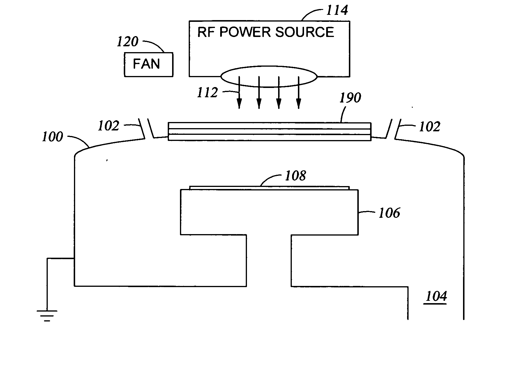
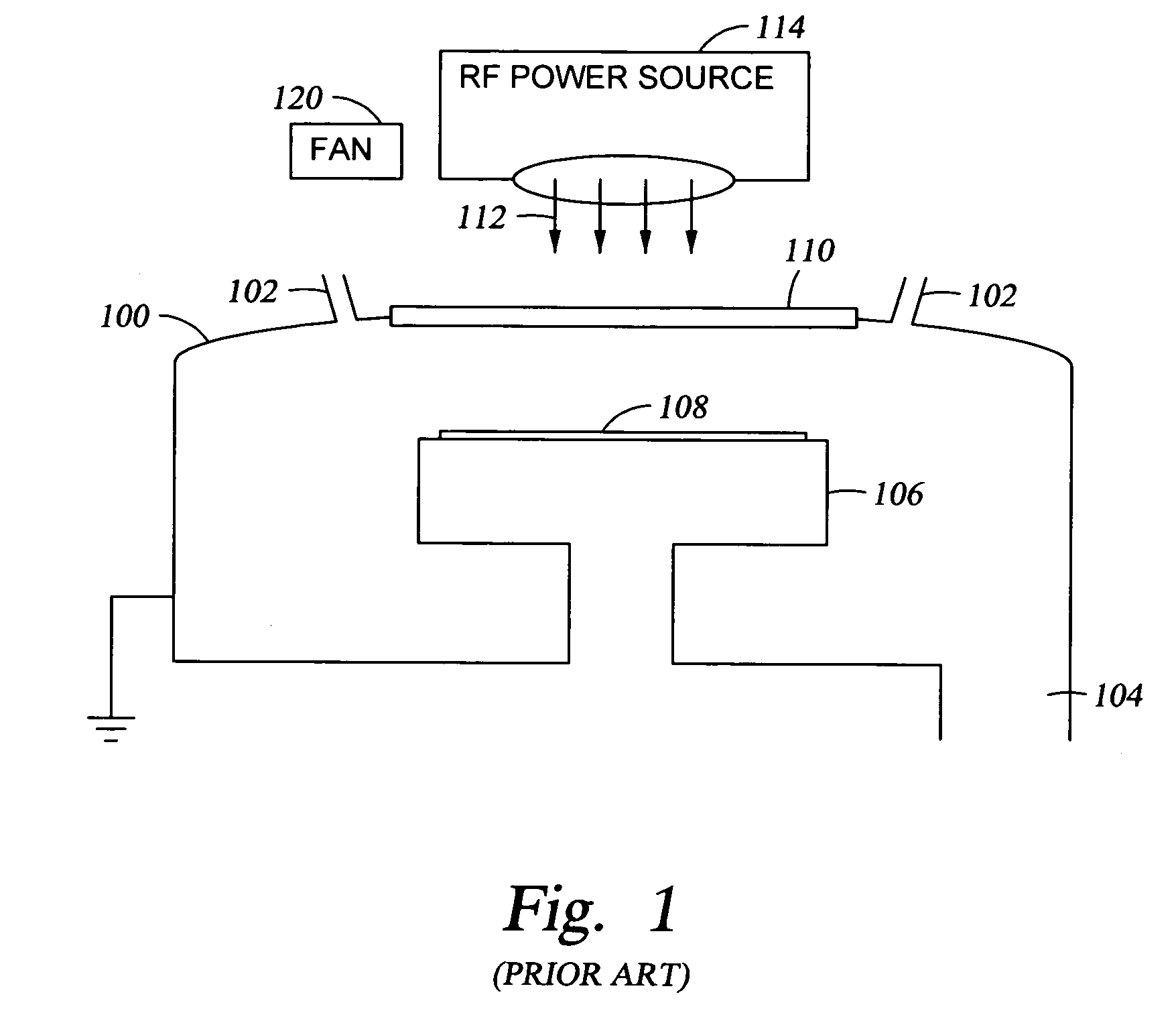
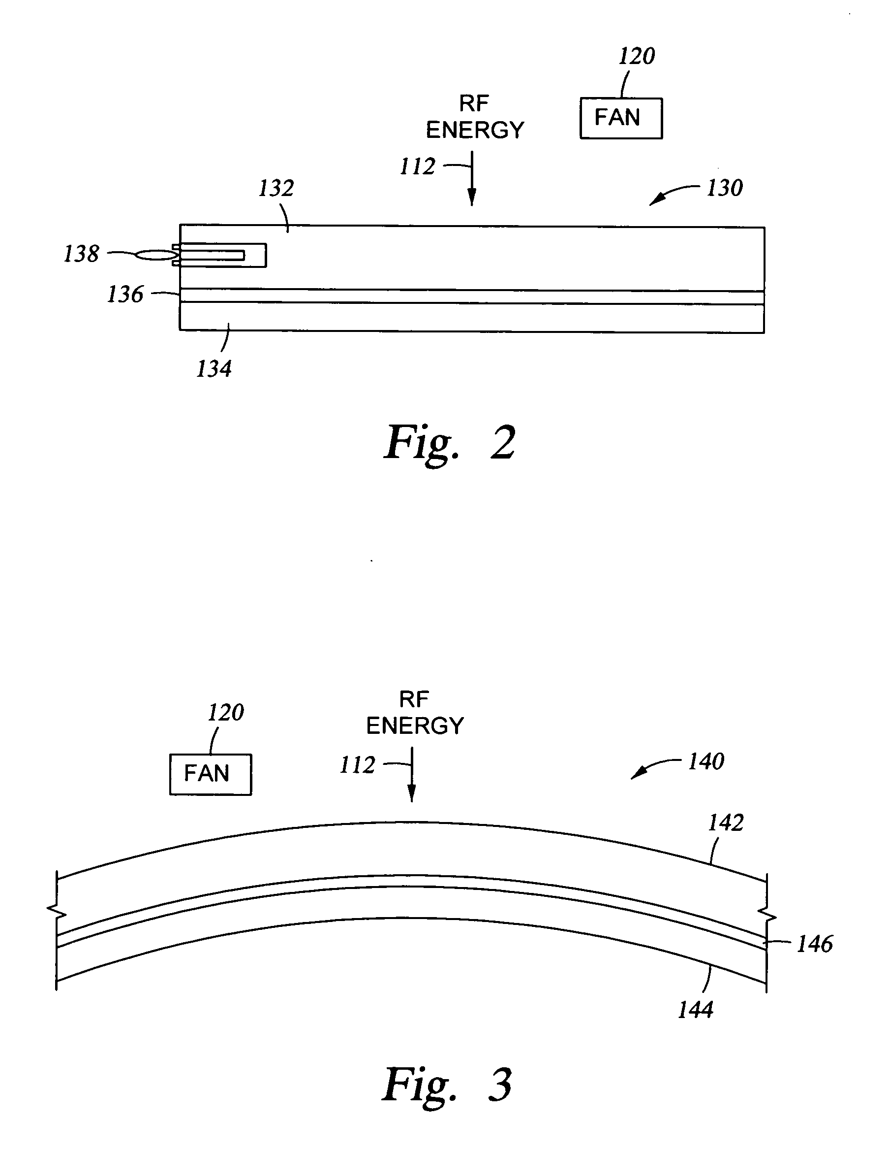
[0029] With reference now to the drawings, FIG. 1 is a simplified cross-sectional side view of a conventional RF plasma reaction chamber presently used for typical processes in the fabrication of integrated circuits in a silicon wafer. The reaction chamber 100 typically includes one or more process gas inlets 102, an exhaust port 104 connected to a vacuum pumping system, and a chuck 106 for supporting a wafer 108 to be processed. The gas inlets 102 may be in the form of a showerhead distributing the process gas over a wide area in opposition to the chuck 106. In one type of an RF plasma reaction chamber, an RF window 110 is disposed in opposition to the chuck 108 to transmit RF energy 112 generated by an RF power source 114, typically operating in the low megahertz range, to the process gases inside the reaction chamber 100. In a typical arrangement, the RF window 110 may be cooled from the outside of the reaction chamber 100. For example, a fan 120 circulates air across the back of...


PUM

PropertyMeasurementUnit
glass forming temperatureaaaaaaaaaa

Abstract

A bonded multi-layer RF window may include an external layer of dielectric material having desired thermal properties, an internal layer of dielectric material exposed to plasma inside a reaction chamber, and an intermediate layer of bonding material between the external layer and the internal layer. Heat produced by the chemical reaction inside the chamber and by the transmission of RF energy through the window may be conducted from the internal layer to the external layer, which may be cooled during a semiconductor wafer manufacturing process. A bonded multi-layer RF window may include cooling conduits for circulating coolant to facilitate cooling of the internal layer; additionally or alternatively, gas distribution conduits and gas injection apertures may be included for delivering one or more process gases into a reaction chamber. A system including a plasma reaction chamber may employ the inventive bonded multi-layer RF window.

Description

RELATED APPLICATION [0001] This application claims priority of provisional application 60 / 721,928, filed Sep. 29, 2005.FIELD OF THE INVENTION [0002] The present invention is related generally to plasma processing chambers, and more particularly to a bonded multi-layer dielectric window which allows coupling of RF energy into a plasma processing chamber. BACKGROUND OF THE INVENTION [0003] Temperature control of the plasma within a radio frequency (RF) plasma reaction chamber has recently become an important factor in achieving and maintaining uniformity in the features produced on silicon wafers processed in such chambers. As wafer densities increase and sub-micron feature sizes continue to decrease, it is becoming more important for critical dimension control to establish predictable and stable plasma temperatures, including temperatures of walls facing and adjacent the plasma, during each process step. Unstable temperature conditions affect the ionization of the gaseous chemicals i...

Claims


Application Information

Patent Timeline
Patent Type & Authority Applications(United States)
IPC IPC(8): B31B1/60C23F1/00C23C16/00
CPCB32B2315/02C04B35/63452C04B37/003C04B37/005C04B37/008C04B2237/10Y10T156/10C04B2237/341C04B2237/343C04B2237/708H01J37/32082H01P1/08C04B2237/34C23C16/4586C23C16/505C23C16/52C23F1/00H01L21/205H01L21/67207
Inventor LI, MAOCHENGHOLLAND, JOHN P.LEAHEY, PATRICK L.QIAN, XUEYUBARNES, MICHAEL S.CLINTON, JONWANG, YOUHAN, NIANCI
Owner APPLIED MATERIALS INC
Why Eureka
Try Eureka