

Semiconductor device
- Summary
- Abstract
- Description
- Claims
- Application Information
AI Technical Summary
Benefits of technology
Problems solved by technology
Method used
Image

Examples
first embodiment
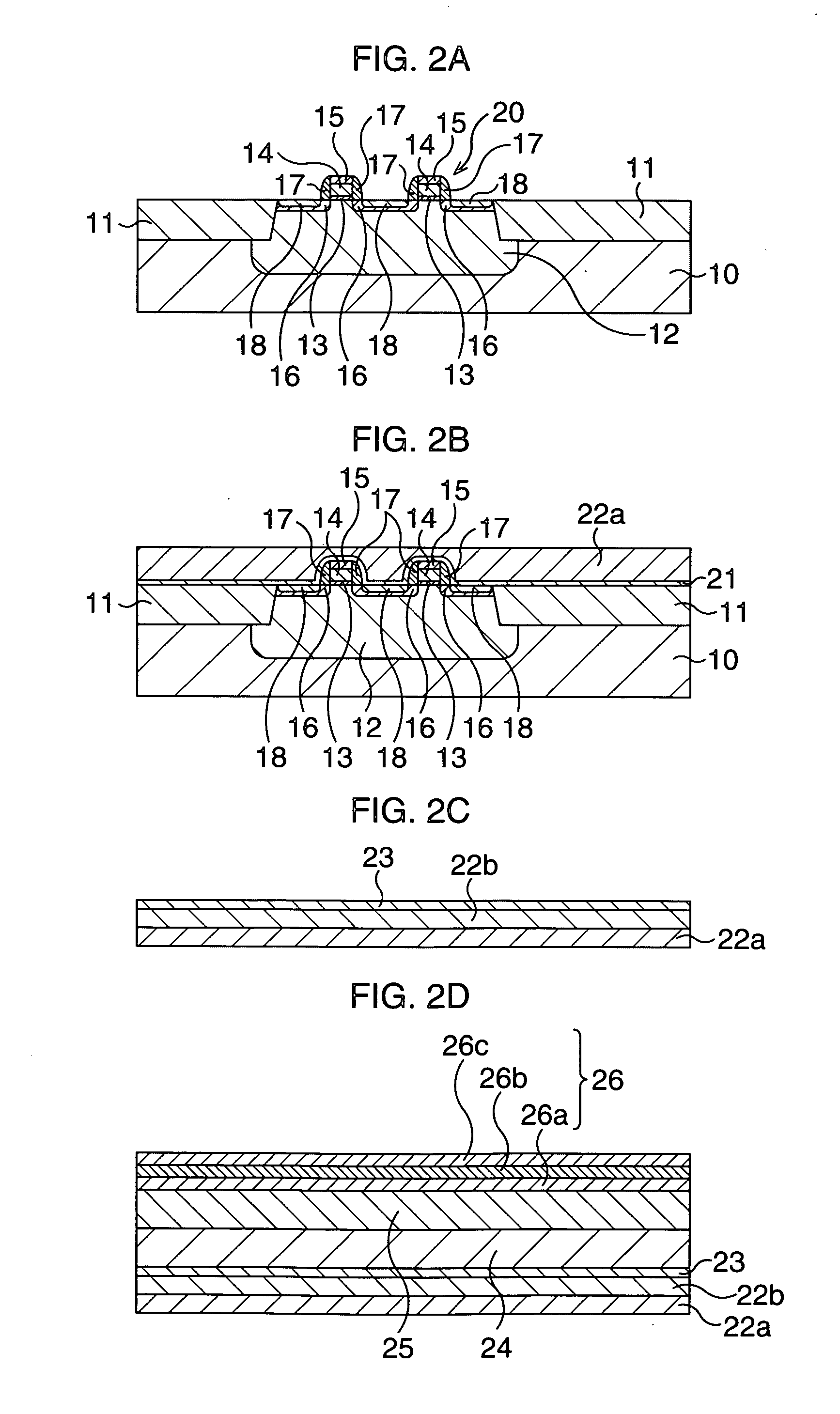
[0149] In this embodiment, a so-called planar type FeRAM will be exemplified, in which conduction of a lower electrode and an upper electrode of a ferroelectric capacitor structure is provided on an upper side of the ferroelectric capacitor structure. Note that for convenience of explanation, the structure of the FeRAM will be described together with a manufacturing method thereof.
[0150]FIG. 2A to FIG. 6B are schematic cross-sectional views showing a structure of an FeRAM according to the first embodiment together with a manufacturing method thereof in the order of steps.
[0151] First, as shown in FIG. 2A, a MOS transistor 20 which functions as a selection transistor is formed on a silicon semiconductor substrate 10.
[0152] Particularly, an element isolation structure 11 is formed on a surface layer of the silicon semiconductor substrate 10 by an STI (Shallow Trench Isolation) method for example to thereby define an element active region.
modification example 12
[0459] In this example, in the structure of the modification example 11, the glue films are formed as a layered structure of a metal film having conductivity even when oxidized and a conductive protection film which inhibits permeation of hydrogen.
[0460]FIG. 30A to FIG. 32B are schematic cross-sectional views showing a structure of an FeRAM according to modification example 12 of the first embodiment together with a manufacturing method thereof (main steps) in the order of steps.
[0461] First, similarly to the first embodiment, the respective steps of FIG. 2A to FIG. 6A are performed.
[0462] Subsequently, as shown in FIG. 30A, an interlayer insulating film 46 is formed so as to cover the first wires 45.
[0463] Particularly, a silicon oxide film is formed with a film thickness of approximately 700 nm so as to cover the first wires 45, and a plasma TEOS film is formed thereon so that a total film thickness thereof is approximately 1100 nm. Thereafter, the surface thereof is polished ...
second embodiment
[0534] In this embodiment, a so-called stack type FeRAM will be exemplified, in which conduction of the lower electrode of a ferroelectric capacitor structure is provided on a lower side of the ferroelectric capacitor structure and conduction of the upper electrode thereof is provided on an upper side of the ferroelectric capacitor structure. Note that for convenience of explanation, the structure of the FeRAM will be described together with a manufacturing method thereof.
[0535]FIG. 38A to FIG. 42B are schematic cross-sectional views showing a structure of an FeRAM according to the second embodiment together with a manufacturing method thereof in the order of steps.
[0536] First, as shown in FIG. 38A, a MOS transistor 220 which functions as a selection transistor is formed on a silicon semiconductor substrate 210.
[0537] Particularly, an element isolation structure 211 is formed on a surface layer of the silicon semiconductor substrate 210 by an STI (Shallow Trench Isolation) metho...
PUM
 Abstract
Description
Claims
Application Information