Method of fabricating a dielectric layer

Inactive Publication Date: 2007-04-12
UNITED MICROELECTRONICS CORP
View PDF4 Cites 3 Cited by
  • Summary
  • Abstract
  • Description
  • Claims
  • Application Information

AI Technical Summary

Benefits of technology

[0032] In addition, since at least one of the annealing processes is performed under the temperature range of equal to or greater than 950° C., it can mend the dielectric surface, which is destroyed by the plasma during the plasma nitridation process.
[0033] In another hand, when the dielectric layer formed in the invention is a gate dielectric layer, the electric performance of the MOS transistor can be improved, including improv

Problems solved by technology

The silicon oxide is therefore not suitable for use as the dielectric layer in the MOS device with more and more reduced size.
However, after the thermal nitridation process, the nitrogen dopants are not uniformly distributed in the dielectric lay

Method used


Image

  • Method of fabricating a dielectric layer
  • Method of fabricating a dielectric layer
  • Method of fabricating a dielectric layer

Examples


Example

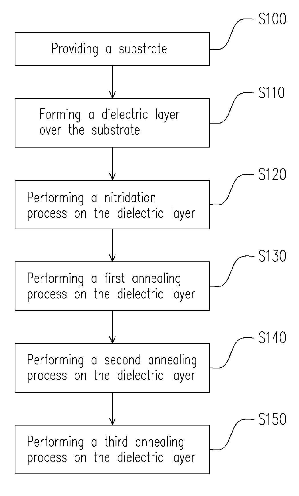
[0039] The invention performs at least two annealing processes on he dielectric layer after performing the nitridation process on the dielectric layer. The nitrogen dopants distributed in the dielectric layer can be uniform when the partial pressure ratio of the inert gas to the oxygen satisfies the following condition.

[0040] At a situation for performing the second annealing process, the first partial pressure ratio (inert gas / oxygen gas) 1for the inert gas to the oxygen gas in the first annealing process is greater than the second partial pressure ratio (inert gas / oxygen gas)2for the inert gas to the oxygen gas in the second annealing process, as follows: (inert gas / oxygen gas)1>(inert gas / oxygen gas) 2.

[0041] At a situation for performing the third annealing process, the first partial pressure ratio (inert gas / oxygen gas) 1for the inert gas to the oxygen gas in the first annealing process is greater than the second partial pressure ratio (inert gas / oxygen gas) 2for the inert ga...


PUM


Abstract

A method of fabricating a dielectric layer is described. A substrate is provided, and a dielectric layer is formed over the substrate. The dielectric layer is performed with a nitridation process. The dielectric layer is performed with a first annealing process. A first gas used in the first annealing process includes inert gas and oxygen. The first gas has a first partial pressure ratio of inert gas to oxygen. The dielectric layer is performed with the second annealing process. A second gas used in the second annealing includes inert gas and oxygen. The second gas has a second partial pressure ratio of inert gas to oxygen, and the second partial pressure ratio is smaller than the first partial pressure ratio. At least one annealing temperature of the two annealing processes is equal to or greater than 950° C. The invention improves uniformity of nitrogen dopants distributed in dielectric layer.

Description

BACKGROUND OF THE INVENTION [0001] 1 . Field of Invention [0002] The present invention relates to the method for fabricating a film layer in a semiconductor device. More particularly, the present invention relates to a method for fabricating a dielectric layer. [0003] 2 . Description of Related Art [0004] When the integration for semiconductor device in integrated circuit is getting larger and larger, it is also requited to have supper-thin gate dielectric layer with high dielectric constant and low leakage current. When the size of a metal oxide semiconductor (MOS) transistor is less than 100 nm, the dielectric constant usually needs to be greater than 7. The material with higher dielectric constant can improve isolation effect. However, the gate dielectric layer in MOS transistor is formed by silicon oxide, and the dielectric constant for the silicon oxide is about 3.9. The silicon oxide is therefore not suitable for use as the dielectric layer in the MOS device with more and more...

Claims


Application Information

Patent Timeline
IPC IPC(8): H01L21/31H01L21/469
CPCH01L21/3144H01L21/022H01L21/0234H01L21/02337H01L21/02332
Inventor WANG, YUN-RENYEN, YING-WEILUNG, CHIEN-HUACHAN, SHU-YENHUANG, KUO-TAI
Owner UNITED MICROELECTRONICS CORP
Why Eureka
Try Eureka