Method of fabricating nitride-based semiconductor laser diode

a laser diode and semiconductor technology, applied in the direction of lasers, semiconductor lasers, laser optical resonators, etc., can solve the problems of catastrophic optical damage, sudden shortening of the life span of the semiconductor laser diode, exponential deformation of optical characteristics, etc., to reduce optical damage and improve characteristics

Inactive Publication Date: 2007-04-19
SAMSUNG ELECTRONICS CO LTD
View PDF7 Cites 11 Cited by
  • Summary
  • Abstract
  • Description
  • Claims
  • Application Information

AI Technical Summary

Benefits of technology

[0017] The present invention can offer a nitride-based semiconductor laser diode designed to reduce optical damage on a ca...

Problems solved by technology

The degradation in optical characteristics occurs exponentially and becomes a major factor leading to abrupt shortening of life span of a semiconductor laser diode.
This is called a ca...

Method used


Image

  • Method of fabricating nitride-based semiconductor laser diode
  • Method of fabricating nitride-based semiconductor laser diode
  • Method of fabricating nitride-based semiconductor laser diode

Examples


Embodiment Construction

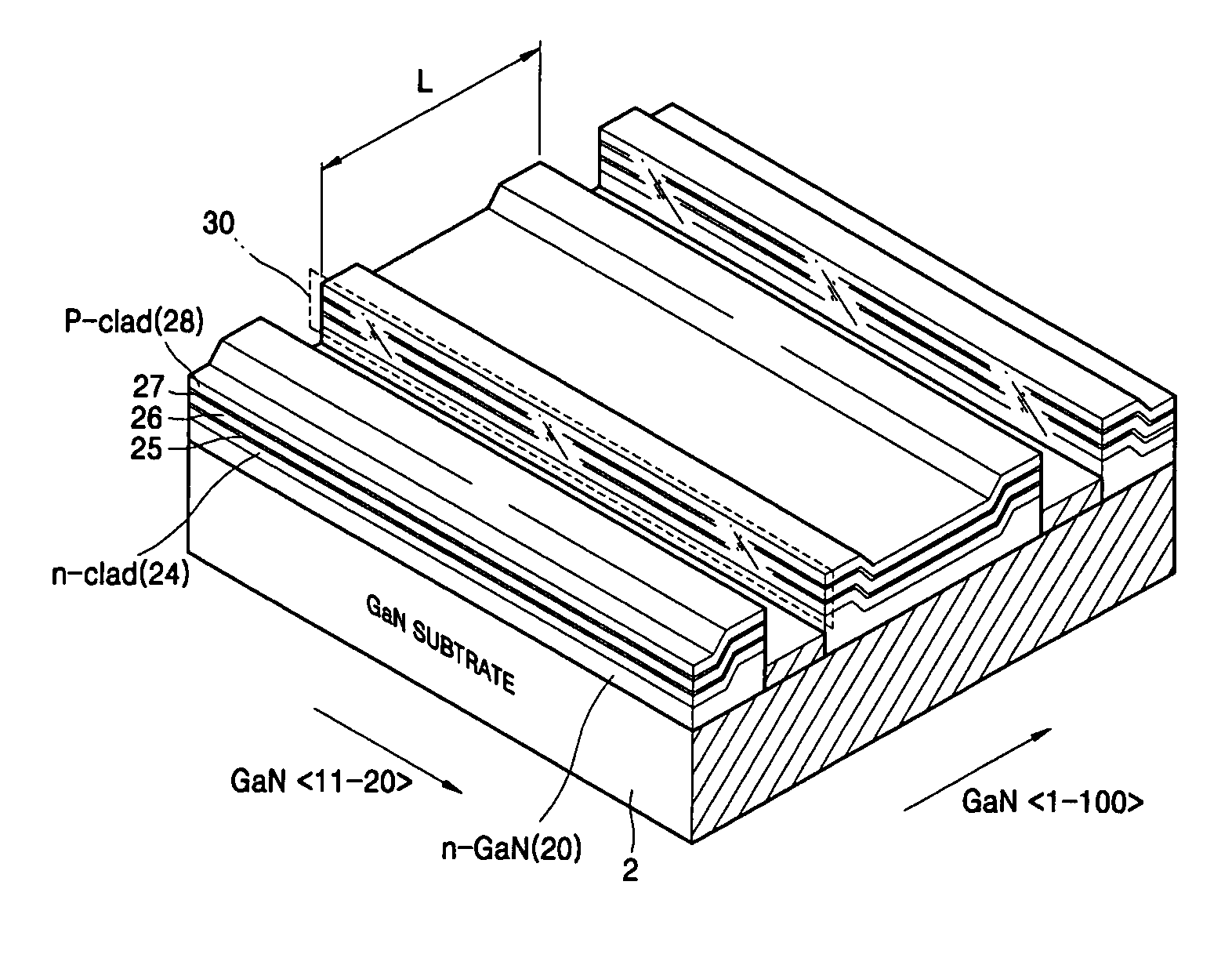
[0023] Hereinafter, methods of manufacturing a nitride-based semiconductor laser diode according to preferred exemplary embodiments of the present invention will be described in detail with reference to accompanying drawings. In the drawings, the thicknesses of layers and regions are exaggerated for clarity.

[0024] Referring to FIG. 1, a nitride-based semiconductor laser diode according to an embodiment of the present invention includes a gallium nitride (GaN) substrate 2, and an n-GaN layer 20, an n-clad layer 24, an n-waveguide layer 25, an active layer 26, a p-waveguide layer 27, and a p-clad layer 28 sequentially formed on the GaN substrate 2.

[0025] The semiconductor laser diode has a laser cavity length L in the GaN direction. Because two (1-100) edges of the n-GaN layer 20 are thicker than other regions thereof, the n-GaN layer 20 has two stepped top edges.

[0026] The n-clad layer 24, the n-waveguide layer 25, the active layer 26, the p-waveguide layer 27, and the p-clad lay...


PUM


Abstract

A method of manufacturing a nitride-based semiconductor laser diode that can minimize optical absorption on a cavity mirror plane and improve the surface roughness of the cavity mirror plane is provided. The method includes the steps of: forming on a (0001) GaN (gallium nitride) substrate having at least two masks spaced apart by a distance equal to a laser cavity length in stripes that extend along the <11-20> direction; growing an n-GaN layer on the GaN substrate between the masks so that two (1-100) edges of the n-GaN layer are thicker than the remaining regions thereof; sequentially stacking an n-clad layer, an active layer, and a p-clad layer on the n-GaN layer to form an edge-emitting laser cavity structure in which laser light generated in the active layer passes through a region of the n-clad layer aligned laterally with the active layer and is output; and etching a (1-100) plane of the laser cavity structure to form a cavity mirror plane.

Description

CROSS-REFERENCE TO RELATED PATENT APPLICATION [0001] This application claims the benefit of Korean Patent Application No. 10-2005-0098724, filed on Oct. 19, 2005, in the Korean Intellectual Property Office, the disclosure of which is incorporated herein in its entirety by reference. BACKGROUND OF THE DISCLOSURE [0002] 1. Field of the Disclosure [0003] The present disclosure relates to a method of fabricating a nitride-based semiconductor laser diode, and more particularly, to a method of manufacturing a nitride-based semiconductor laser diode that can minimize optical absorption on a cavity mirror plane and improve the surface roughness of the cavity mirror plane. [0004] 2. Description of the Related Art [0005] In an edge-emitting semiconductor laser diode, when laser light emerges from an exit surface, the semiconductor crystalline structure on the exit surface is distorted due to high photon density and Joule heating, thereby increasing optical absorption and laser threshold curre...

Claims


Application Information

Patent Timeline
IPC IPC(8): H01L21/00
CPCB82Y20/00H01S5/0213H01S5/16H01S5/22H01S5/2201H01S5/34333H01S2304/12H01S5/30
Inventor SAKONG, TANSUNG, YOUN-JOONPAEK, HO-SUN
Owner SAMSUNG ELECTRONICS CO LTD
Why Eureka
Try Eureka