Method for fabricating thin film transistors
- Summary
- Abstract
- Description
- Claims
- Application Information
AI Technical Summary
Benefits of technology
Problems solved by technology
Method used
Image

Examples
Embodiment Construction
[0035] Reference will now be made in detail to the present preferred embodiments of the invention, examples of which are illustrated in the accompanying drawings. Wherever possible, the same reference numbers are used in the drawings and the description to refer to the same or like parts.
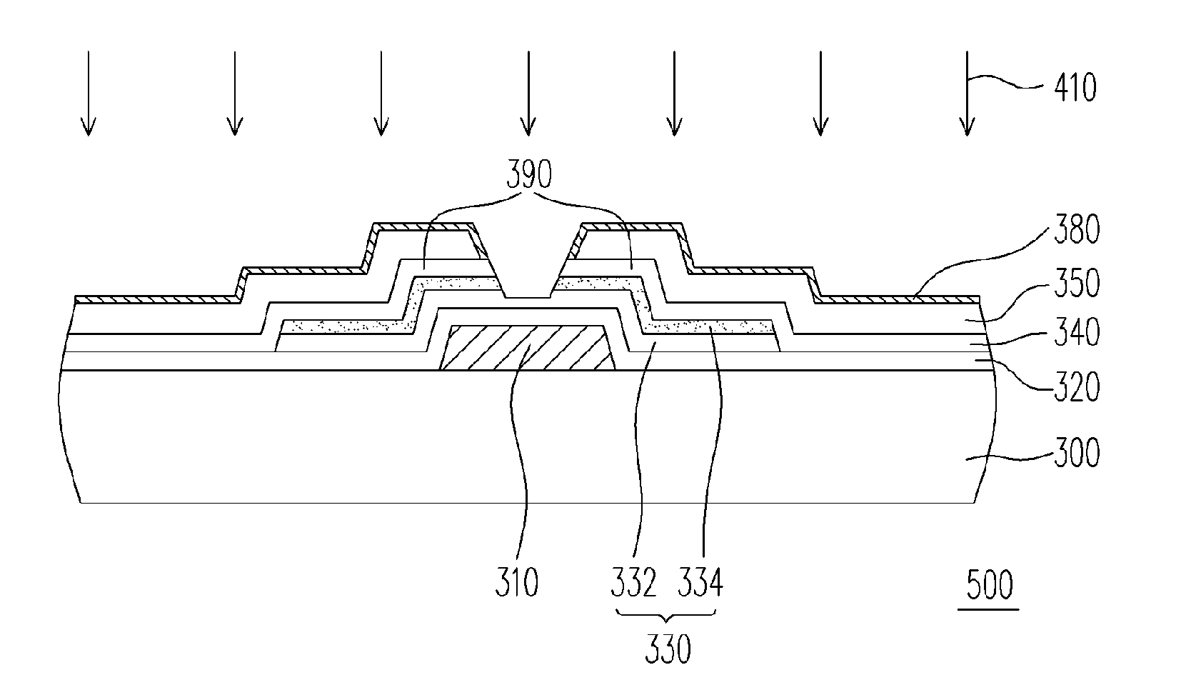
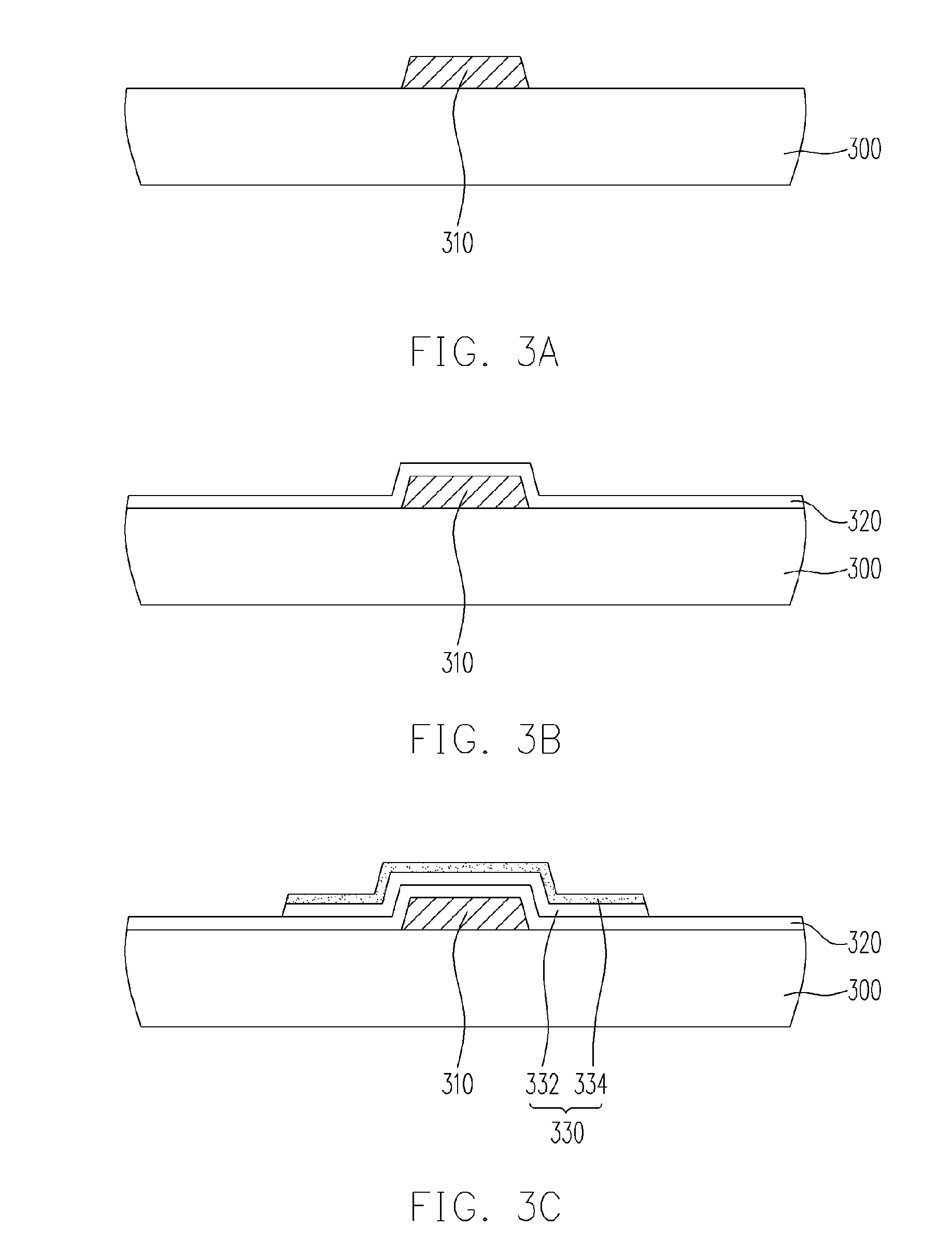
[0036]FIGS. 3A through 3J are schematic cross-sectional views showing the steps for fabricating a thin film transistor according to one preferred embodiment of the present invention. First, a gate 310 is formed on a substrate 300 as shown in FIG. 3A. In one embodiment of the present invention, the method of forming the gate 310 is described in FIGS. 4A through 4E. First, as shown in FIG. 4A, a first conductive layer 210 and a second conductive layer 220 are sequentially formed on the substrate 300. The method of forming the conductive layer 210 and 220 includes, for example, performing a sputtering or an evaporation process. The conductive layer 210 is fabricated using a low contact resistant, high...
PUM
 Abstract
Description
Claims
Application Information
 - Generate Ideas
- Intellectual Property
- Life Sciences
- Materials
- Tech Scout
- Unparalleled Data Quality
- Higher Quality Content
- 60% Fewer Hallucinations
Browse by: Latest US Patents, China's latest patents, Technical Efficacy Thesaurus, Application Domain, Technology Topic, Popular Technical Reports.
© 2025 PatSnap. All rights reserved.Legal|Privacy policy|Modern Slavery Act Transparency Statement|Sitemap|About US| Contact US: help@patsnap.com