Method for manufacturing semiconductor device
Active Publication Date: 2007-05-03
MICRON TECH INC
21 Cites 57 Cited by
AI-Extracted Technical Summary
Problems solved by technology
However, short channel effects in a transistor become more severe as the gate length is shortened, and drawbacks occur whereby sub-threshold current increases.
When the substrate impurity concentration is increased in order to minimize this effect, deterioration of the refresh character...
View moreBenefits of technology
[0019] According to the present invention, a gate trench is formed in the memory cell region, and then a second gate insulating film that is thicker than the first gate insulating film is formed on the inner wall of the gate trench in a state in which the first gate insulating film on the peripheral circuit region is covered by a protective film. The first gate insulating film and the second gate insulating film can therefore be formed independently of each other. Accordingly, the number of oxidation steps performed in the gate trench can be reduced. Oxidation stress in the gate trench can thereby be reduced, and a degradation of the refresh characteristics can be prevented. Since the first gate insulating film and the second gate insulating film are formed independently rather than simultaneously, the film thickness and other characteristics are easily controlled. ...
View moreAbstract
A method for manufacturing a semiconductor device whereby the process is simplified and high performance can be obtained in both a trench-gate transistor and a planar transistor that has a thin gate insulating film when the two transistors are formed on the same semiconductor substrate. In a state in which the gate insulating film (11s) in a peripheral circuit region PE is covered by a protective film (12), a gate trench (18) is formed in a memory cell region M, after which a gate insulating film (19) that is thicker than the gate insulating film (11s) is formed on an inner wall of the gate trench (18) in a state in which the gate insulating film (11s) of the peripheral circuit region PE is still covered by the protective film (12).
Application Domain
Technology Topic
Image
Examples
- Experimental program(2)
Example
First Embodiment
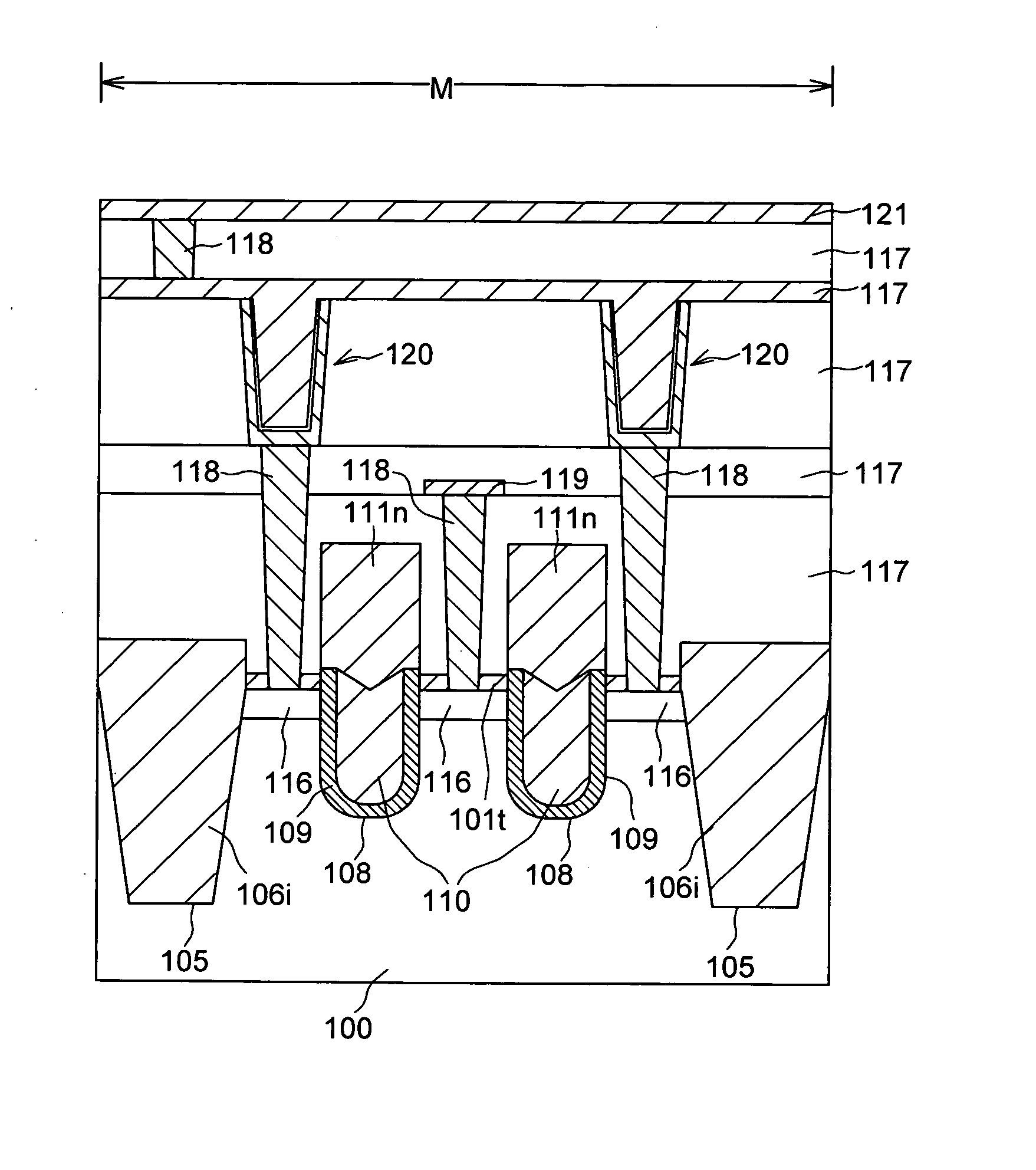
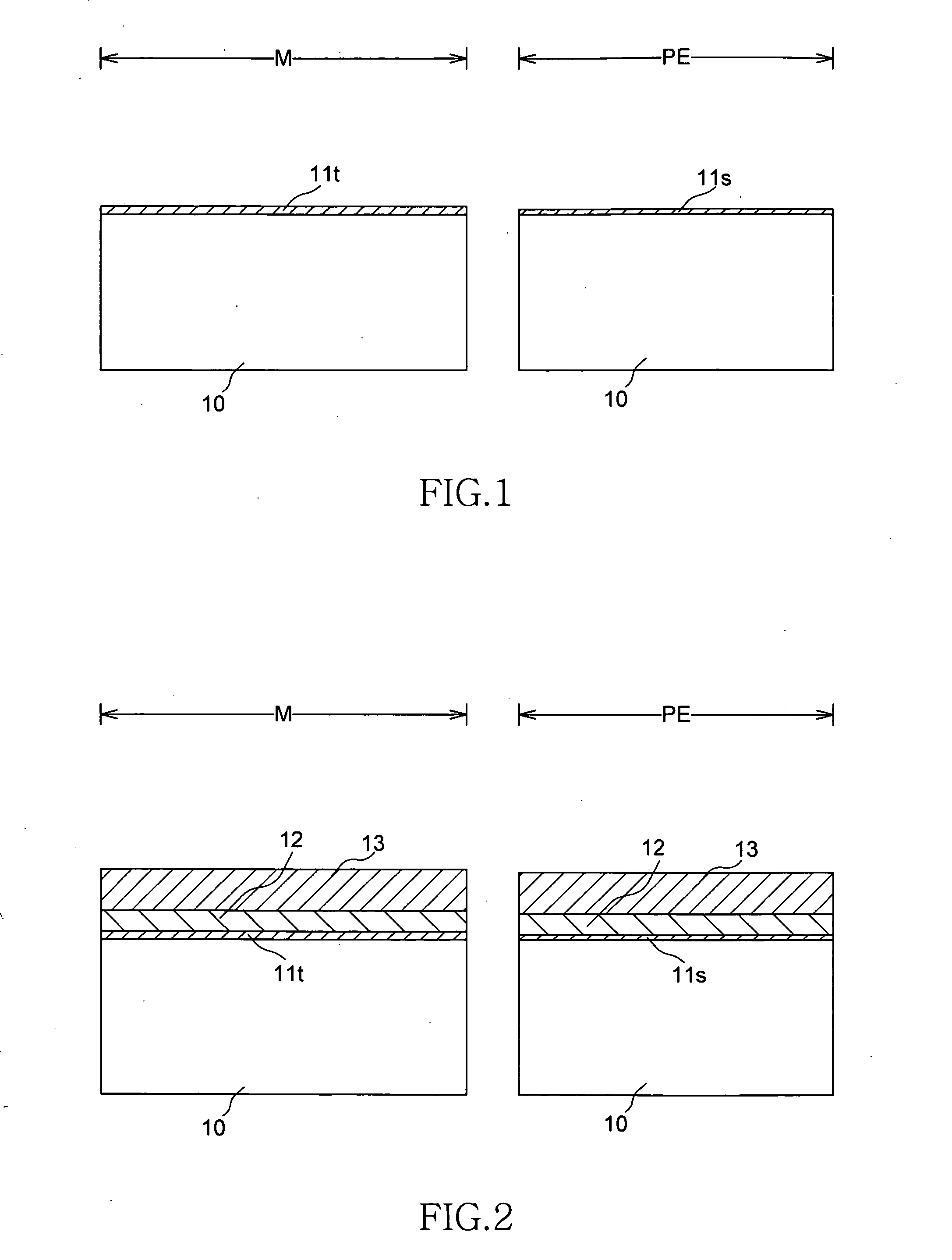
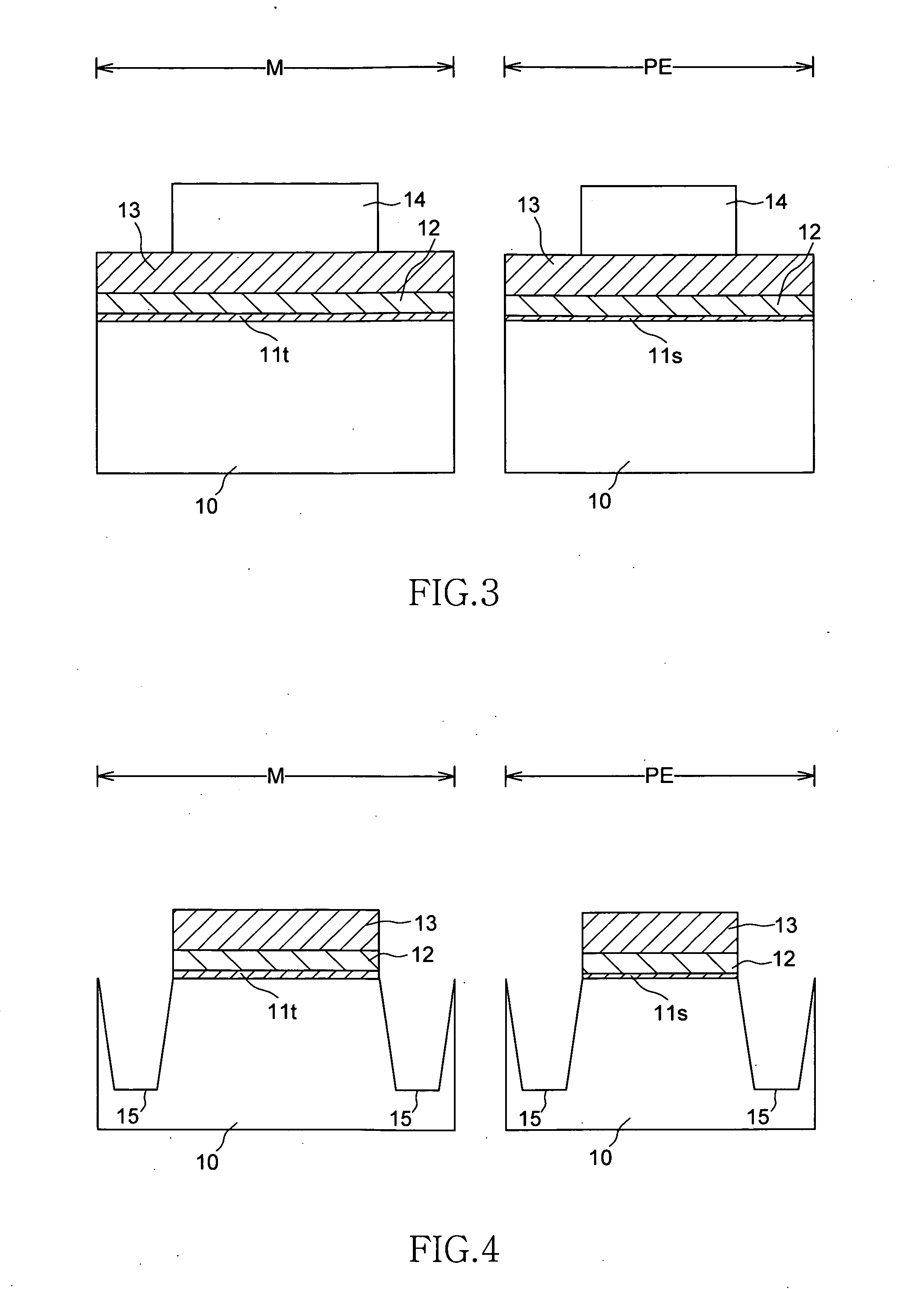
[0067]FIGS. 1 through 18 are schematic views showing the process for manufacturing a semiconductor device that has a trench-gate transistor and a planar transistor according to a first embodiment of the present invention. In FIGS. 1 through 18, “region M” indicates the memory cell region in which the trench-gate transistor is formed, and “region PE” indicates the peripheral circuit region in which the planar transistor is formed.
[0068] First, a thin oxide film 11s having a thickness of approximately 1.5 to 3 nm is formed on the surface of region PE of a semiconductor substrate 10, as shown in FIG. 1. A thick oxide film 11t having a thickness of approximately 4.5 to 6 nm is also formed in region M and in a region (not shown) in which a power supply circuit and the like are formed, and which is a region other than region PE of the peripheral circuit region. In a specific example, a thermal oxide film having a thickness of slightly less than 6 nm is formed on the entire surface of the semiconductor substrate 10 by thermal oxidation, the region other than region PE is covered by a resist mask, and the thermal oxide film on region PE is removed, after which the resist mask is removed, and the entire surface of the substrate 10 is cleaned with an acid. This cleaning removes a portion of the surface of the thermal oxide film on region M and on the region (not shown) in which a power supply circuit and the like are formed, and the thickness of the thermal oxide film is reduced to about 5 nm. Then, the entire surface is again thermal-oxidized to form a thin oxide film 11s having a thickness of about 3 nm on region PE, and a thick oxide film lit having a thickness of about 6 nm on region M and the region (not shown) in which a power supply circuit and the like are formed. The thin oxide film 11s thereby formed is the gate insulating film of the planar transistor formed in region PE.
[0069] The thickness of the oxide film lit formed in region M herein may be equal to that of the thin oxide film 11s. However, the oxide film lit in region M is preferably formed thick as described above so that in a case in which the gate electrode of the trench-gate transistor formed in region M is formed in a shape that protrudes further than the surface of the semiconductor substrate 10, even when the protruding portion is misaligned with respect to the gate trench 18, high breakdown voltage can be maintained in the misaligned portion as well. The thick oxide film 11t is also the gate insulating film of a transistor having a high breakdown voltage that is formed in a region (not shown) in which a power supply circuit and other components are formed.
[0070] In the subsequent step as shown in FIG. 2, a phosphorus-doped amorphous silicon film 12 as a protective film that has a thickness of approximately 10 to 30 nm is then formed by a CVD (Chemical Vapor Deposition) method in order to protect the thin oxide film 11s. A silicon nitride film 13 having a thickness of approximately 80 to 150 nm is then formed by an LP (Low Pressure)-CVD method.
[0071] As shown in FIG. 3, a resist pattern 14 is formed on each element separation region formed as a region for separating elements according to the STI (Shallow Trench Isolation) technique.
[0072] As shown in FIG. 4, after the silicon nitride films 13 are patterned using the resist patterns 14 as a mask, and the resist patterns 14 are then removed, the phosphorus-doped amorphous silicon films 12, the thick oxide films 11t, the thin oxide films 11s, and the semiconductor substrate 10 are dry-etched using the patterned silicon nitride films 13 as masks. The phosphorus-doped amorphous silicon films 12, the thick oxide films 11t, and the thin oxide films 11s are thereby patterned, and trenches 15 used for STI are also formed in the semiconductor substrate 10.
[0073] A thermal oxidation treatment is then performed in order to remove the etching damage from the inner walls of the trenches 15, after which silicon oxide films 16 are formed on the entire surface by an HDP (High-Density Plasma)-CVD method so as to fill in the trenches 15, as shown in FIG. 5.
[0074] CMP (Chemical Mechanical Polishing) is then performed using the silicon nitride films 13 as a stopper, the silicon oxide films 16 on the silicon nitride films 13 are removed by polishing so that the silicon oxide films 16 remain in the trenches 15. Element separation regions 16i are thereby formed, as shown in FIG. 6.
[0075] As shown in FIG. 7, a resist pattern 17 that is provided with a plurality of openings is then formed on region M in order to form the gate trenches of the trench-gate memory cell transistor in region M. Region PE is completely covered at this time by resist patterns 17. Openings are also formed in the resist pattern 17 above the element separation regions 16i of region M in order to be used for a gate trench that is formed in an adjacent memory cell region (not shown).
[0076] Using the resist pattern 17 as a mask, the silicon nitride film 13 is then patterned in the shape of the mask, as shown in FIG. 8.
[0077] After the resist pattern 17 is removed, the phosphorus-doped amorphous silicon film 12 and the thick oxide film 11t are etched, and the semiconductor substrate 10 is also etched, whereby gate trenches 18 are formed in the semiconductor substrate 10, as shown in FIG. 9. The silicon nitride film 13 that was used as a mask for forming the STI trenches 15 shown in FIG. 4 thus remains without being removed, and is also used as a mask for forming the gate trenches 18, as shown in FIG. 9.
[0078] Sacrificial oxidation is then performed by thermal oxidation to remove damage and contamination from the etched surfaces inside the gate trenches 18, and the sacrificial oxide film is then removed by wet etching. A silicon oxide film 19 is then formed to act as the gate insulating film of the memory cell transistor, as shown in FIG. 10. This silicon oxide film 19 must also have high voltage resistance as described above, and preferably has a thickness of approximately 4.5 to 6 nm. The silicon oxide film 19 herein is preferably formed by a process in which a CVD oxide film (preferably a HTO (High Temperature Oxide)) having a thickness of approximately 3.5 to 5.5 nm is deposited by a CVD method at a temperature of approximately 800° C., after which the CVD oxide film is thermally oxidized at a temperature of approximately 1050° C. in order to densify the CVD oxide film, remove impurities, and modify the interface between the CVD oxide film and the semiconductor substrate 10. The time needed to form the second gate insulating film in the gate trench can thereby be prevented from increasing even when further reduction in size narrows the opening of the gate trench, and an increase in oxidation stress can also be suppressed.
[0079] In contrast, when the full-thickness portion of the silicon oxide film 19 is formed by thermal oxidation, not only is the oxidation time lengthened, but oxidizing species also diffuse into the interface between the semiconductor substrate 10 and the element separation regions (STI) 16i. This causes a cubical expansion because the STI 16i are oxidized, thereby creating stress in the semiconductor substrate 10 and adversely affecting the junction characteristics of the DRAM. Accordingly, the silicon oxide film 19 is preferably formed according to the method described above. At this time, since the thin oxide film 11s formed on the semiconductor substrate 10 in region PE is covered by the phosphorus-doped amorphous silicon film 12 that is the protective film, it is possible to prevent a CVD oxide film from being deposited on the thin oxide film 11s, and to prevent the thin oxide film 11s from becoming thicker as a result of thermal oxidation.
[0080] In order to form the gate electrode of the trench-gate transistor, an amorphous silicon film that is doped with phosphorus as an N-type impurity is then formed on the entire surface that includes the insides of the gate trenches 18. Phosphorus-doped amorphous silicon films 20 are then embedded in the gate trenches 18 as shown in FIG. 11, by performing a planarization process according to a CMP method in which the silicon nitride film 13 is used as a stopper.
[0081] The phosphorus-doped amorphous silicon films 20 in the gate trenches 18 are then etched back to about the same position as the thick oxide film 11t by dry etching, as shown in FIG. 12.
[0082] Wet etching is then performed to remove the silicon nitride film 13, the upper portions of the element separation regions 16i, and the upper portions of the silicon oxide films 19. The upper surfaces of the element separation regions 16i and the phosphorus-doped amorphous silicon film 12 are thereby aligned with each other, as shown in FIG. 13. In this arrangement, the phosphorus-doped amorphous silicon film 12 is formed on the gate insulating film 11s in region PE, and is made to function as a protective film when the nitride film 13 (see FIG. 12) used as a mask for forming the gate trench 18 is removed. It is therefore possible to prevent the gate insulating film 11s from being damaged.
[0083] A CVD method is then used to form an amorphous silicon film (phosphorus-doped amorphous silicon film) 21 that is doped with phosphorus as an N-type impurity and has a thickness of approximately 30 to 80 nm on the entire surface, as shown in FIG. 14.
[0084] A resist pattern 22 used to form a gate electrode is then formed on the phosphorus-doped amorphous silicon film 21, as shown in FIG. 15.
[0085] The phosphorus-doped amorphous silicon film 21 is then patterned using a resist pattern 22 as a mask, as shown in FIG. 16. A gate electrode of a trench-gate transistor composed of the phosphorus-doped amorphous silicon films 20 and 21 is thereby formed in region M, and a gate electrode of a planar transistor composed of the phosphorus-doped amorphous silicon films 12 and 21 is formed in region PE.
[0086] The example described herein is of a case in which the patterned amorphous silicon films 21 are not misaligned with respect to the gate trenches 18 in region M. However, when misalignment does occur, the amorphous silicon films 21 remain on the thick oxide film lit and become portions of a gate electrode. In this type of case, the thick oxide film 11t functions as a portion of the gate insulating film in this trench-gate transistor. However, since the oxide film t is formed so as to have about the same thickness as the silicon oxide films 19 in the gate trenches 18, a reduction in the breakdown voltage thereof can be minimized.
[0087] N-type source/drain diffusion regions 23 are formed in region M, and N-type source/drain diffusion regions 24 are formed in region PE by ion implantation of an N-type impurity into regions M and PE using each gate electrode as a mask, as shown in FIG. 17. A trench-gate memory cell transistor is thereby formed in region M, and a planar transistor is formed in region PE.
[0088] The amorphous silicon films 12, 20 and 21 are converted from amorphous silicon films to polycrystalline silicon films by the heat treatment performed to activate the source/drain diffusion regions, or by a subsequent heating process.
[0089] Various types of wiring or cell capacitors are then layered in region M using a common method. Specifically, DRAM having a trench-gate memory cell transistor is formed by a process in which an interlayer insulating film 25 is formed on the memory cell transistor, and a contact plug 26 that pass through the interlayer insulating film 25, a bit line 27, a cell capacitor 28, Al wiring 29, and other components are formed, as shown in FIG. 18.
[0090] In the present embodiment as described above, a thin oxide film 11s is formed in advance to function as the gate insulating film of the planar transistor on the semiconductor substrate 10 of the peripheral circuit region PE, and this thin oxide film 11s is covered by the amorphous silicon film 12. In this state, a gate trench 18 is formed in memory cell region M, and a gate insulating film 19 that is thicker than the gate insulating film 11s is formed on the inner wall of the gate trench 18. Since the amorphous silicon film 12 thereby functions as a protective film for preventing growth of the gate insulating film 11s, the gate insulating film 19 can be made thick while the gate insulating film 11s remains thin. Specifically, the gate insulating film 11s and the gate insulating film 19 can be formed independently of each other. The number of oxidation steps performed in the gate trench 18 can therefore be reduced.
[0091] According to the present embodiment, oxidation stress in the gate trench 18 can be reduced, and a degradation of the refresh characteristics can be prevented. Since the gate insulating film 11s and the gate insulating film 19 are formed independently rather than simultaneously, the film thickness and other characteristics are easily controlled.
Example
Second Embodiment
[0092] As a second embodiment, an example will next be described in which the present invention is applied when a trench-gate transistor having a thick oxide film as the gate insulating film is formed in the memory cell region in the same manner as in the first embodiment, and a dual-gate-structured transistor having a thin oxide film as the gate insulating film is formed in the peripheral circuit region. In a dual-gate structure, a gate electrode that includes N-type polycrystalline silicon into which an N-type impurity (phosphorus or the like) is introduced is used as the gate electrode of an N-channel transistor, and a gate electrode that includes P-type polycrystalline silicon into which a P-type impurity (boron or the like) is introduced is used in a P-channel transistor.
[0093]FIGS. 19 through 38 are schematic views showing the process for manufacturing a semiconductor device that has a trench-gate transistor and a dual-gate-structured transistor according to a second embodiment of the present invention. In FIGS. 19 through 38, “region M” indicates the memory cell region in which the trench-gate transistor is formed, and “region P” and “region N” are provided to the peripheral circuit region, wherein “region P” is a region (also referred to as a P-type peripheral circuit region) in which a planar P-channel transistor provided with a gate electrode that includes P-type polycrystalline silicon is formed, and “region N” is a region (also referred to as an N-type peripheral circuit region) in which a planar N-channel transistor provided with a gate electrode that includes N-type polycrystalline silicon is formed.
[0094] First, a thin oxide film 101s having a thickness of approximately 1.5 to 3 nm is formed on the surface of regions P and N of a semiconductor substrate 100, as shown in FIG. 19. A thick oxide film 101t having a thickness of approximately 4.5 to 6 nm is also formed in region M and in a region (not shown) in which a power supply circuit and the like are formed, and which is a region other than region P or N of the peripheral circuit region. Specifically, the thin oxide film 101s and the thick oxide film 101t are formed in the same manner as the thin oxide film 11s and the thick oxide film t in the process shown in FIG. 1 in the abovementioned first embodiment. The thin oxide film 101s thus formed is the gate insulating film of a dual-gate-structured planar transistor formed in regions P and N.
[0095] The thickness of the oxide film 101t formed in region M may be the same as that of the thin oxide film 101s, but a thick film is preferred for the same reason as in the first embodiment. The thick oxide film 101t is the gate insulating film of a transistor having a high breakdown voltage that is formed in a region (not shown) in which a power supply circuit and other components are formed, the same as the thick oxide film 11t in the first embodiment.
[0096] In the subsequent step as shown in FIG. 20, a non-doped amorphous silicon film 102 as a protective film that has a thickness of approximately 10 to 30 nm is then formed by a CVD (Chemical Vapor Deposition) method in order to protect the thin oxide film 101s. In the present embodiment, since a dual-gate-structured transistor is formed in regions P and N of the peripheral circuit region, a non-doped amorphous silicon film is used as the protective film instead of the doped amorphous silicon film used in the abovementioned first embodiment. A silicon nitride film 103 having a thickness of approximately 80 to 150 nm is then formed by an LP (Low Pressure)-CVD method.
[0097] As shown in FIG. 21, a resist pattern 104 is formed on each element separation region formed as a region for separating elements according to the STI (Shallow Trench Isolation) technique.
[0098] As shown in FIG. 22, after the silicon nitride films 103 are patterned using the resist patterns 104 as a mask, and the resist patterns 104 are then removed, the non-doped amorphous silicon films 102, the thick oxide films 101t, the thin oxide films 101s, and the semiconductor substrate 100 are dry-etched using the patterned silicon nitride films 103 as masks. The non-doped amorphous silicon films 102, the thick oxide films 101t, and the thin oxide films 101s are thereby patterned, and trenches 105 used for STI are also formed in the semiconductor substrate 100.
[0099] A thermal oxidation treatment is then performed in order to remove the etching damage from the inner walls of the trenches 105, after which silicon oxide films 106 are formed on the entire surface by an HDP (High-Density Plasma)-CVD method so as to fill in the trenches 105, as shown in FIG. 23.
[0100] CMP (Chemical Mechanical Polishing) is then performed using the silicon nitride films 103 as a stopper, the silicon oxide films 106 on the silicon nitride films 103 are removed by polishing so that the silicon oxide films 106 remain in the trenches 105. Element separation regions 106i are thereby formed, as shown in FIG. 24.
[0101] As shown in FIG. 25, a resist pattern 107 that is provided with a plurality of openings is then formed on region M in order to form the gate trenches of the trench-gate memory cell transistor in region M. Regions P and N are completely covered at this time by resist patterns 107.
[0102] Using the resist pattern 107 as a mask, the silicon nitride film 103 is then patterned in the shape of the mask, as shown in FIG. 26.
[0103] After the resist pattern 107 is removed, the non-doped amorphous silicon film 102 and the thick oxide film 101t are etched, and the semiconductor substrate 100 is also etched, whereby gate trenches 108 are formed in the semiconductor substrate 100, as shown in FIG. 27. The silicon nitride film 103 that was used as a mask for forming the STI trenches 105 shown in FIG. 22 thus remains without being removed, and is also used as a mask for forming the gate trenches 108, as shown in FIG. 27.
[0104] Sacrificial oxidation is then performed by thermal oxidation to remove damage and contamination from the etched surfaces inside the gate trenches 108, and the sacrificial oxide film is then removed by wet etching. A silicon oxide film 109 is then formed to act as the gate insulating film of the memory cell transistor, as shown in FIG. 28. This silicon oxide film 109 is the gate insulating film of the memory cell transistor, and therefore must have a high breakdown voltage, as in the first embodiment, and the thickness thereof is preferably about B 4.5 to 6 nm. This silicon oxide film 109 can be formed in the same manner as the silicon oxide film 19 formed in the steps of the first embodiment shown in FIG. 10. The thin oxide film 101s formed on the semiconductor substrate 100 of regions P and N is covered at this time by a non-doped amorphous silicon film 102, which is a protective film. It is therefore possible to prevent an oxide film from being further deposited on the thin oxide film 101s, and to prevent the thin oxide film 101s from increasing in thickness due to thermal oxidation.
[0105] In order to form the gate electrode of the trench-gate transistor, an amorphous silicon film that is doped with phosphorus as an N-type impurity is then formed on the entire surface that includes the insides of the gate trenches 108. Phosphorus-doped amorphous silicon films 110 are then embedded in the gate trenches 108 as shown in FIG. 29, by performing a planarization process according to a CMP method in which the silicon nitride film 103 is used as a stopper.
[0106] The phosphorus-doped amorphous silicon films 110 in the gate trenches 108 are then etched back to about the same position as the thick oxide film 101t by dry etching, as shown in FIG. 30.
[0107] Wet etching is then performed to remove the silicon nitride film 103, the upper portions of the element separation regions 106i, and the upper portions of the silicon oxide films 109. The upper surfaces of the element separation regions 106i and the protective film (non-doped amorphous silicon film) 102 are thereby aligned with each other, as shown in FIG. 31.
[0108] A CVD method is then used to form a non-doped amorphous silicon film 111 having a thickness of approximately 30 to 80 nm to become the gate electrode of the dual-gate transistor, as shown in FIG. 32. Also unlike the abovementioned first embodiment, a dual-gate-structured transistor is formed in regions P and N in the present embodiment. A non-doped amorphous silicon film is therefore used instead of a doped amorphous silicon film as the film for forming the gate electrode.
[0109] As shown in FIG. 33, regions M and N are then masked by a resist pattern 112, and boron (B) as a P-type impurity is ion-implanted into region P. This ion implantation of boron is performed at a low energy of 10 keV or less. The implanted boron ions are diffused in a subsequently performed heat treatment, whereby the non-doped amorphous silicon films 111 and 102 (see FIG. 32) of region P become P-type amorphous silicon films 111p and 102p.
[0110] After the resist pattern 112 is removed, region P in this instance is masked by a resist pattern 113, and phosphorus (P) as an N-type impurity is ion-implanted into regions M and N, as shown in FIG. 34. This ion implantation of phosphorus is also performed at a low energy of 20 keV or less, the same as the ion implantation of boron described above, and the phosphorus ions are diffused by a subsequent heat treatment. The non-doped amorphous silicon films 111 and 102 (see FIG. 33) of region N thereby become N-type amorphous silicon films 111n and 102n. The non-doped amorphous silicon films 111 and 102 of region M are also made into N-type amorphous silicon films 111n and 102n by this ion implantation.
[0111] According to the present embodiment, phosphorus-doped silicon films 110 are already embedded in the gate trenches 108 of region M. Ion implantation can therefore be performed under suitable implantation conditions according to the thickness of the silicon film 111 and the silicon film 102 without regard to implantation into the gate trenches 108 when ion implantation into region M is performed at the same time as phosphorus is implanted into region N in the ion implantation process for creating P-type and N-type non-doped silicon films 111, which are the gate electrodes of the dual-gate transistor.
[0112] Resist patterns 114 for use in forming gate electrodes are then formed on the impurity-doped amorphous silicon films 111n and 111p, as shown in FIG. 35.
[0113] As shown in FIG. 36, the layered film that includes the amorphous silicon films 111p and 102p, as well as the layered film that includes the amorphous silicon films 111n and 102n, are then each patterned using the resist pattern 114 as a mask. A gate electrode of a trench-gate transistor composed of doped amorphous silicon films 110 and 111n is thereby formed in region M, a P-type gate electrode composed of doped amorphous silicon films 111p and 102p is formed in region P, and an N-type gate electrode composed of doped amorphous silicon films 111n and 102n is formed in region N.
[0114] As shown in FIG. 37, regions M and N are then covered by a resist film (not shown), and P-type source/drain diffusion regions 115p are formed by ion-implanting a P-type impurity into region P using the P-type gate electrode as a mask. Region P is then covered by a resist film (not shown), and an N-type impurity is ion-implanted into regions M and N using the gate electrodes of regions M and N as masks. N-type source/drain diffusion regions115n are thereby formed in region N, and N-type source/drain diffusion regions 116 are formed in region M. According to this process, a trench-gate memory cell transistor is formed in region M, and a dual-gate transistor is formed in regions P and N, which are peripheral circuit regions.
[0115] The amorphous silicon films 111n, 111p, 102p, 102n, and 110 are converted from amorphous silicon films to polycrystalline silicon films by the heat treatment performed to activate the source/drain diffusion regions, or by a subsequent heating process.
[0116] Various types of wiring or cell capacitors are then layered in region M using a common method similar to the first embodiment. Specifically, DRAM having a trench-gate memory cell transistor is formed by a process in which an interlayer insulating film 117 is formed on the memory cell transistor, and a contact plug 118 that pass through the interlayer insulating film 117, a bit line 119, a cell capacitor 120, Al wiring 121, and other components are formed, as shown in FIG. 38.
[0117] According to the present embodiment as described above, a thin oxide film 101s is formed in advance on the semiconductor substrate 100 of regions P and N in the peripheral circuit region to become the gate insulating film of the dual-gate-structured transistor that is formed in regions P and N. A gate trench 108 is then formed in the memory cell region M in a state in which the thin oxide film 101s is covered by an amorphous silicon film 102, and a gate insulating film 109 that is thicker than the gate insulating film 101s is formed on the inner wall of the gate trench 108, whereby the gate insulating film 101s and the gate insulating film 109 can be formed independently of each other. The same effects as those of the abovementioned first embodiment are thereby obtained.
[0118] Furthermore, according to the present embodiment, an amorphous silicon film 110 that is selectively doped with an impurity can be formed in the gate trench 108 of region M. Specifically, the following processes are involved in an example of a possible method for selectively forming doped silicon in the gate trench when a trench-gate transistor and a dual-gate-structured transistor are formed on the same substrate. After a gate trench is formed in a semiconductor substrate, a thermal oxide film serving as the gate insulating film of the transistors is formed in the gate trench and on the semiconductor substrate in the peripheral circuit region in which the dual-gate-structured transistor is formed, and a doped silicon film is formed on the entire surface that includes the inside of the gate trench. The doped silicon film is then etched back so as to remain only in the gate trench, a non-doped silicon film is formed on the gate insulating film to be used for the gate electrode of the dual-gate-structured transistor, and P- and N-type gate electrodes are each formed by ion implantation.
[0119] However, in this method, the gate insulating film of the dual-gate-structured transistor is usually damaged when the doped silicon is etched back, making it difficult to form a high-performance transistor. In the present embodiment, however, a non-doped amorphous silicon film 102 is formed on the gate insulating film 101s on regions P and N, which are the regions in which the dual-gate-structured transistor is formed, in the step for removing the silicon nitride film 103 that is used as a mask for forming the gate trench 108, the gate insulating film 109, the doped silicon film 110 that is embedded in the gate trench 108, and the gate trench 108. Damage to the gate insulating film 101s can thereby be prevented when the mask nitride film 103 is removed.
[0120] Accordingly, it is possible to form an impurity-doped amorphous silicon film 110 in the gate trench 108, and to form a non-doped amorphous silicon film 111 on regions P and N as well as on the doped amorphous silicon film 110 that was embedded in the gate trenches. The silicon films 110, 111, and 102 can thereby be formed in the appropriate impurity concentrations without damaging the gate insulating film 101s, and the trench-gate transistor and the dual-gate-structured transistor can both be endowed with high performance.
[0121] As described above, an amorphous silicon film 110 that is selectively doped with an impurity can be formed in the gate trench 108. Depletion of the trench-gate electrode can thereby be prevented in contrast to a case in which an impurity is introduced after a non-doped silicon film is formed in the gate trench.
[0122] The present invention is in no way limited to the aforementioned embodiments, but rather various modifications are possible within the scope of the invention as recited in the claims, and naturally these modifications are included within the scope of the invention.
[0123] For example, in the abovementioned embodiments, the protective film used for covering the thin oxide film 11s (101s) was a doped amorphous silicon film 12 in the first embodiment, and a non-doped amorphous silicon film 102 in the second embodiment. However, these configurations are not limiting, and another material may also be used insofar as the resulting film can prevent an oxide film from being layered on the thin oxide film 11s (101s) when the gate insulating film 19 (109) is formed in the gate trench 18 (108), or thickness from being increased due to further oxidation, while the operation of the transistors is not impeded. Specifically, another material may be used insofar as the resulting film (conductive thin film or the like) allows formation of a channel needed during the application of voltage to a gate electrode.
[0124] In the abovementioned embodiment, an example was described in which each silicon film was first formed in an amorphous state and then converted to a polycrystalline silicon film by a subsequent heating process. However, polycrystalline silicon films may also be used initially as needed.
[0125] In the embodiments described above, a layered film that included silicon films 12 (102) and 21 (111) was used as the gate electrode of the planar transistor, but the silicon film 12 (102), which is a protective film, may be formed in advance so as to initially have the required thickness as a gate electrode in cases in which the gate trench 108 or the STI trench 15 (105) has a small depth, and in other cases.
[0126] The gate electrode is also not necessarily formed using only silicon films, and it is also possible to form a silicide layer on a silicon film, or to create a so-called polymetal gate electrode by layering metal films.
[0127] Furthermore, the example described above was one in which the mask layer for forming the trenches 15 (105) that were used for STI, and the mask layer for forming the gate trenches 18 (108) were used in common in the silicon nitride film 13 (103). However, the silicon nitride film 13 (103) may be removed after the STI (element separation regions) 16i (106i) are formed, and a new silicon nitride film may be created to form a mask layer.
Login to view more PUM


Description & Claims & Application Information
We can also present the details of the Description, Claims and Application information to help users get a comprehensive understanding of the technical details of the patent, such as background art, summary of invention, brief description of drawings, description of embodiments, and other original content. On the other hand, users can also determine the specific scope of protection of the technology through the list of claims; as well as understand the changes in the life cycle of the technology with the presentation of the patent timeline. Login to view more.
Login to view more Similar technology patents
Grouper breeding heat stress resisting method
ActiveCN110800653AReduce oxidative stressImprove adaptabilityClimate change adaptationAnimal feeding stuffAntioxidative stressGrouper
Owner:HAINAN CHENHAI AQUATIC CO LTD
Protein sugar-control meal replacement powder and preparation method thereof
PendingCN112262989AReduce oxidative stressReduce inflammationFood scienceNutrientDiabetic complication
Owner:光翰科技(上海)有限公司
Composition containing cannabidiol for treating nerve tinnitus and preparation method of composition
InactiveCN110201030AReduce oxidative stressRepair the auditory nerveSenses disorderOrganic chemistryGlycerolAuditory nerves
Owner:李卫
Antioxidant compounds and methods of their use
Owner:QUEENSLAND UNIVERSITY OF TECH
Composition for preparing burn and wound dressing as well as preparation and preparation method thereof
PendingCN114748683AReduce oxidative stressRestore repair functionBandagesMoisture retentionBurn wound
Owner:SHENZHEN BAY LAB
Classification and recommendation of technical efficacy words
- Prevent degradation
- Reduce oxidative stress
Protective coating materials for electrochromic devices
InactiveUS6204953B1Prevent degradationThin material handlingNon-linear opticsPolycarbonatePoly(benzimidazole)
Owner:OPTICAL COATING LAB
Coated implantable medical device
Owner:COOK MEDICAL TECH LLC
Dipeptidyl peptidase IV inhibitors and methods of making and using dipeptidyl peptidase IV inhibitors
InactiveUS20040152745A1Effectively competePrevent degradationBiocideOrganic compound preparationCentral nervous systemProstate
Owner:GUILFORD PHARMACEUTICALS INC
Gamma correction method, gamma correction apparatus, and image reading system
ActiveUS7271939B2Reduce memory capacityPrevent degradationImage enhancementDigitally marking record carriersCorrection methodImaging data
Owner:SEIKO EPSON CORP
Frequency and resolution analyzed biometric authentication method and device
InactiveUS7099495B2Prevent degradationAdequate authentication precisionImage analysisUser identity/authority verificationImage resolutionIris image
Owner:PANASONIC CORP
Dietary supplement
InactiveUS20120003378A1Reduce oxidative stressReduce plaqueBiocideOrganic chemistryRHODIOLA ROSEA ROOTToxin
Owner:RBC LIFE SCI
Method of improving hair quality by improving scalp health
PendingUS20170135932A1Good for healthReduce oxidative stressCosmetic preparationsHair cosmeticsSurface energyHair streams
Owner:THE PROCTER & GAMBLE COMPANY
Haematococcus pluvialis astaxanthin product formula assisting in infertility treatment
InactiveCN107536055AReduce oxidative stressImprove quality and vitalityFood scienceMotilityChemistry
Owner:HANGZHOU XINWEI LOW CARBON TECH R&D
Cortex moutan linear alpha-D-1,4-glucan as well as preparation method and application thereof
ActiveCN113480677AReduce oxidative stressSmall molecular weightOrganic active ingredientsMetabolism disorderGlucanMolecular biology
Owner:QINGDAO UNIV OF SCI & TECH
Grouper breeding heat stress resisting method
ActiveCN110800653AReduce oxidative stressImprove adaptabilityClimate change adaptationAnimal feeding stuffAntioxidative stressGrouper
Owner:HAINAN CHENHAI AQUATIC CO LTD