Accessible chip stack and process of manufacturing thereof

Inactive Publication Date: 2007-05-03
ALSEPHINA INNOVATIONS INC
View PDF6 Cites 176 Cited by
  • Summary
  • Abstract
  • Description
  • Claims
  • Application Information

AI Technical Summary

Benefits of technology

[0010] In effect, the access to wiring for the integrated circuits or semiconductor devices is provided through upper chips towards chips positioned therebelow, so as to be adhesively bonded together and whereby usual planar wafer design, bonding, dicing and handling can be implemented, and in which the upper chips commence with SOI or the like technologies so as to be readily capable of being thinned, as necessary. This particular thinning process effectively affords that any through-vias in the chip can be of reasonable dimensions and are built or formed while the wafers are s

Problems solved by technology

However, although this patent is directed to a method of stacking ultra thin chips with interconnections for maximizing the operational speed of an integrated circuit package, there is no disclos

Method used


Image

  • Accessible chip stack and process of manufacturing thereof
  • Accessible chip stack and process of manufacturing thereof
  • Accessible chip stack and process of manufacturing thereof

Examples


Embodiment Construction

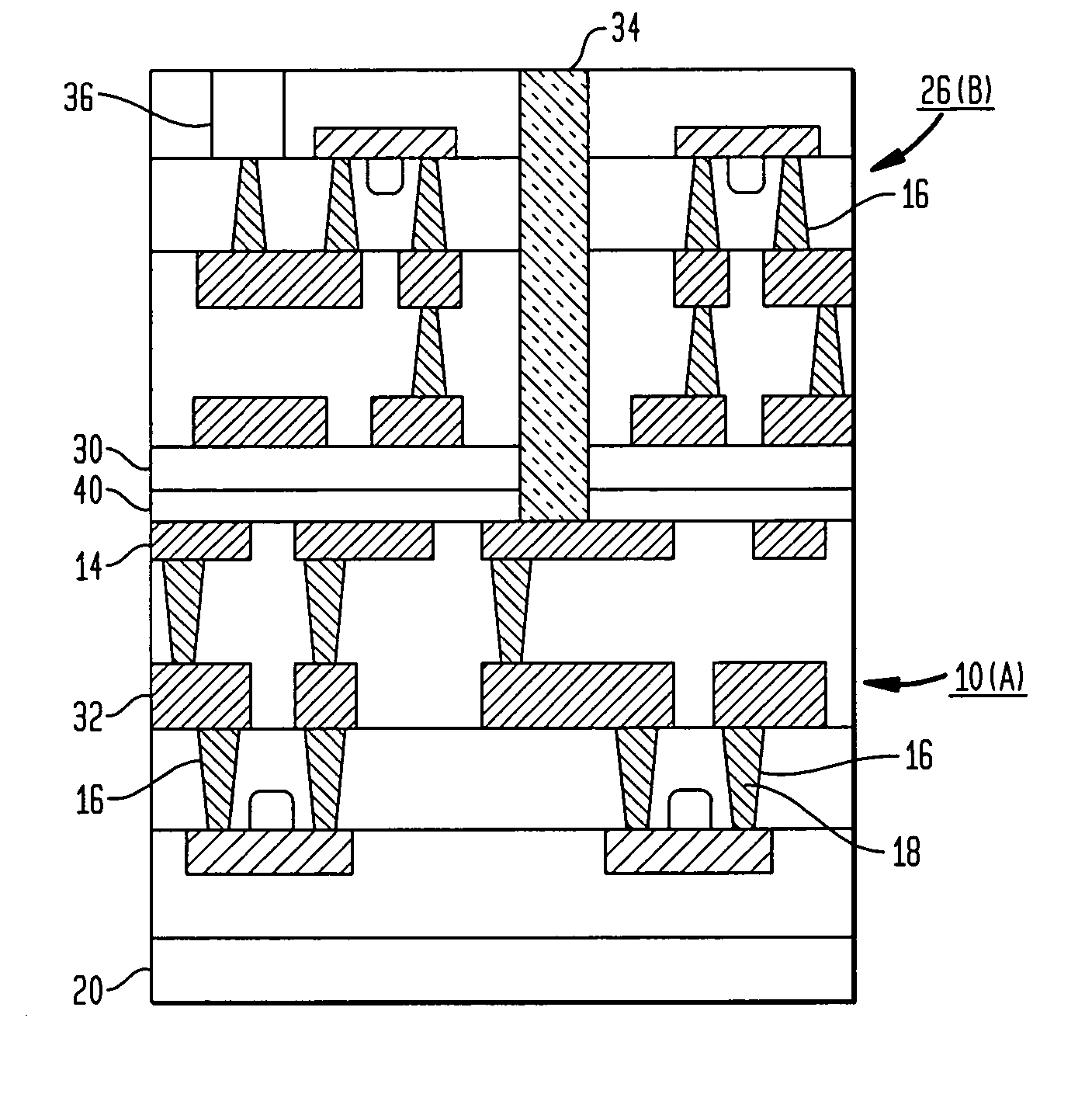
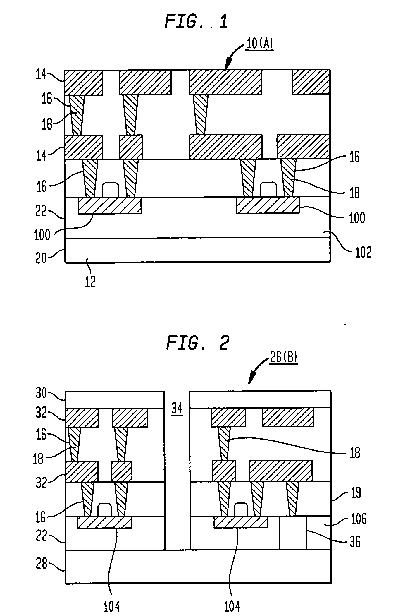
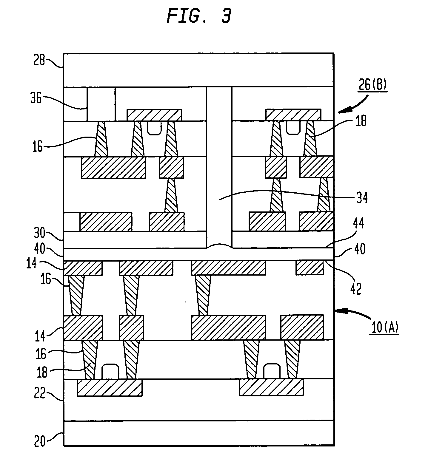
[0021] Referring in specific detail to the drawings, as shown in FIG. 1, there is provided a first base semiconductor Chip 10 (identified as A), which is arranged on a substrate, such as a planar wafer 12, and is provided with a plurality of metal levels 14, of which only two are illustrated in this particular embodiment, although additional levels and layers may be readily provided for multiple-level technologies. Also provided in base semiconductor Chip 10 are, for example, active devices including Field Effect Transistor (FET) gate electrodes 100 and active SOI regions 102.

[0022] This particular chip structure is in a wafer form, and includes interconnecting passages and vias 16 filled with electrically conductive material 18, as may be required by a specific technology. The chip is mounted on a handle 20 constituting a handling layer below a Buried Oxide (“BOX”) and Shallow Trench Isolation (“STI”) layer 22, and will remain permanently thereon. Hereby, the chip can be bulk, Si,...


PUM


Abstract

A process of manufacturing a three-dimensional integrated circuit chip or wafer assembly and, more particularly, a processing of chips while arranged on a wafer prior to orienting the chips into stacks. Also disclosed is the manufacture of the three-dimensional integrated circuit wherein the chip density can be very high and processed while the wafers are still intact and generally of planar constructions.

Description

BACKGROUND OF THE INVENTION [0001] 1. Field of the Invention [0002] The present invention relates to a process of manufacturing a three-dimensional integrated circuit chip or wafer assembly and, more particularly, relates to the processing of chips while arranged on a wafer prior to orienting the chips into stacks. Furthermore, the invention also pertains to the manufacture of the three-dimensional integrated circuit wherein the chip density can be very high and processed while the wafers are still intact and generally of planar constructions. [0003] In essence, the basic concept of forming three-dimensional or stacked integrated circuits is well known in the semiconductor and related technology, in which the use and fabrication of multi-chip stacks are widely employed in enabling multiple and diverse technologies, and materials can be readily combined into a single system in order to provide functions which are incapable of being obtained by means of single technology and material ...

Claims


Application Information

Patent Timeline
IPC IPC(8): H01L29/40H01L21/44
CPCH01L21/76898H01L23/481H01L25/0657H01L25/50H01L2225/06513H01L2225/06541H01L2225/06596H01L2224/32145H01L2224/9202H01L2924/0002H01L29/40
Inventor FURUKAWA, TOSHIHARUHAKEY, MARK C.HOLMES, STEVEN J.HORAK, DAVID V.KOBURGER, CHARLES W. III
Owner ALSEPHINA INNOVATIONS INC
Why Eureka
Try Eureka