Bias circuit for BJT amplifier

a bias circuit and amplifier technology, applied in the field of bias circuits, can solve the problems of degrading the linearity of the amplifier circuit, delaying the demodulation of the signal, etc., and achieve the effect of reducing the odd-order intermodulation distortion and improving the efficiency of reducing the conduction angle operation

Active Publication Date: 2007-05-03
WJ COMM
View PDF14 Cites 41 Cited by
  • Summary
  • Abstract
  • Description
  • Claims
  • Application Information

AI Technical Summary

Benefits of technology

[0011] In some embodiments, the power-amplifying device includes at least one BJT device, and the bias circuit employs BJT components so that the current-mirror serves two functions simultaneously. One function is to provide a current-mirror or level-shifting operation required for setting and controlling the quiescent conditions for the BJT in the power-amplifying device. The second function is to respond to the modulation envelope in the input RF signal by rectifying each negative half cycle in the input RF signal. The charge accumulated in each negative half cycle is deposited in the bypass capacitor and a properly amplified and delayed version of this charge is returned back through

Problems solved by technology

For communication systems involving a modulated carrier signal whose modulation frequency is a small fraction of the carrier frequency, odd-order intermodulation distortion (IMD) processes are the primary sources of deleterious signal distortion in power amplifiers.
Furthermore, BJT operation at high power (e.g., 2-10 W) and high voltage (e.g., >10V) requires substantial thermal ballasting in either or both of the base and emitter terminals of the power-amplifying transistor.
Such thermal ballasting h

Method used


Image

  • Bias circuit for BJT amplifier
  • Bias circuit for BJT amplifier
  • Bias circuit for BJT amplifier

Examples


Embodiment Construction

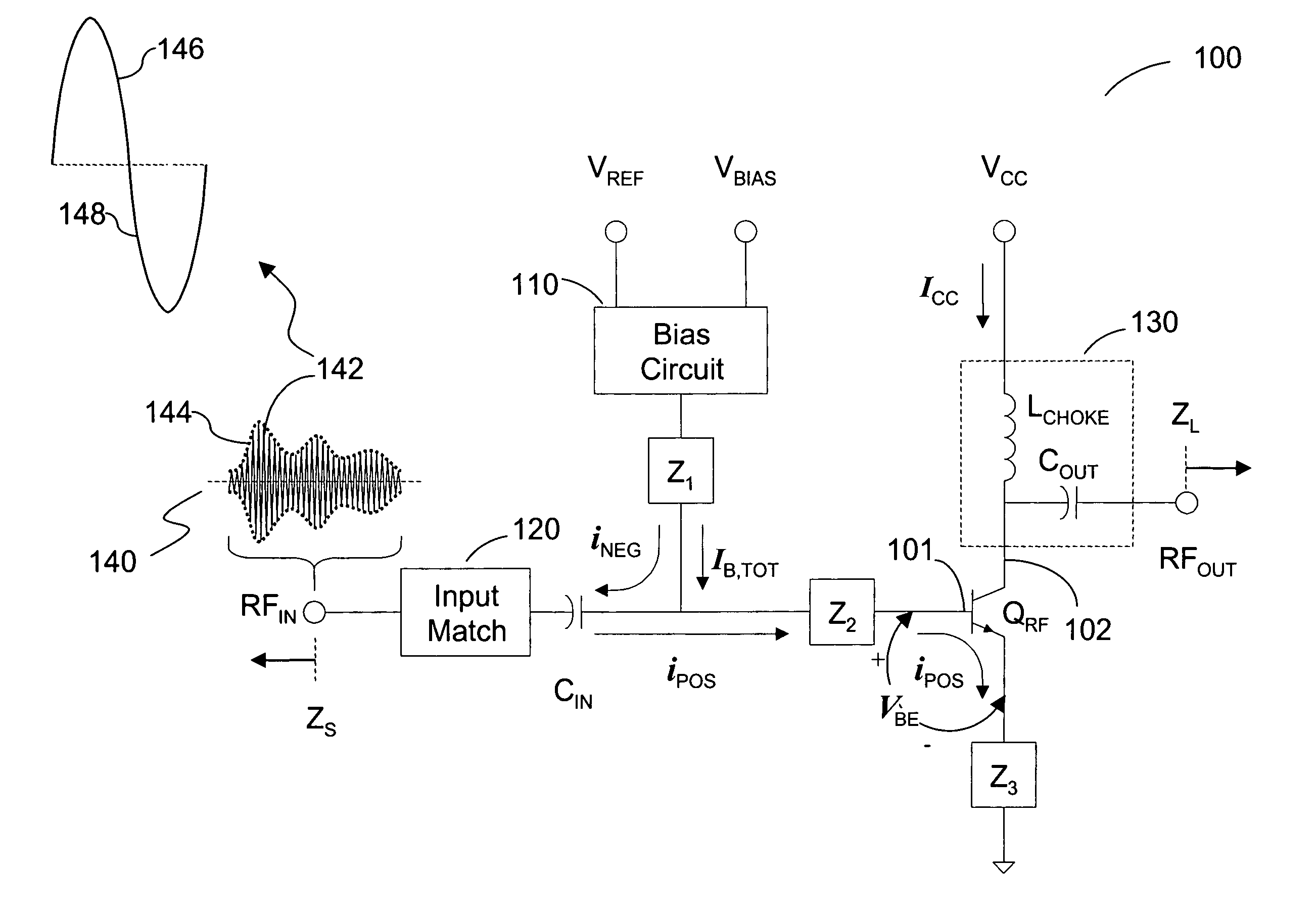
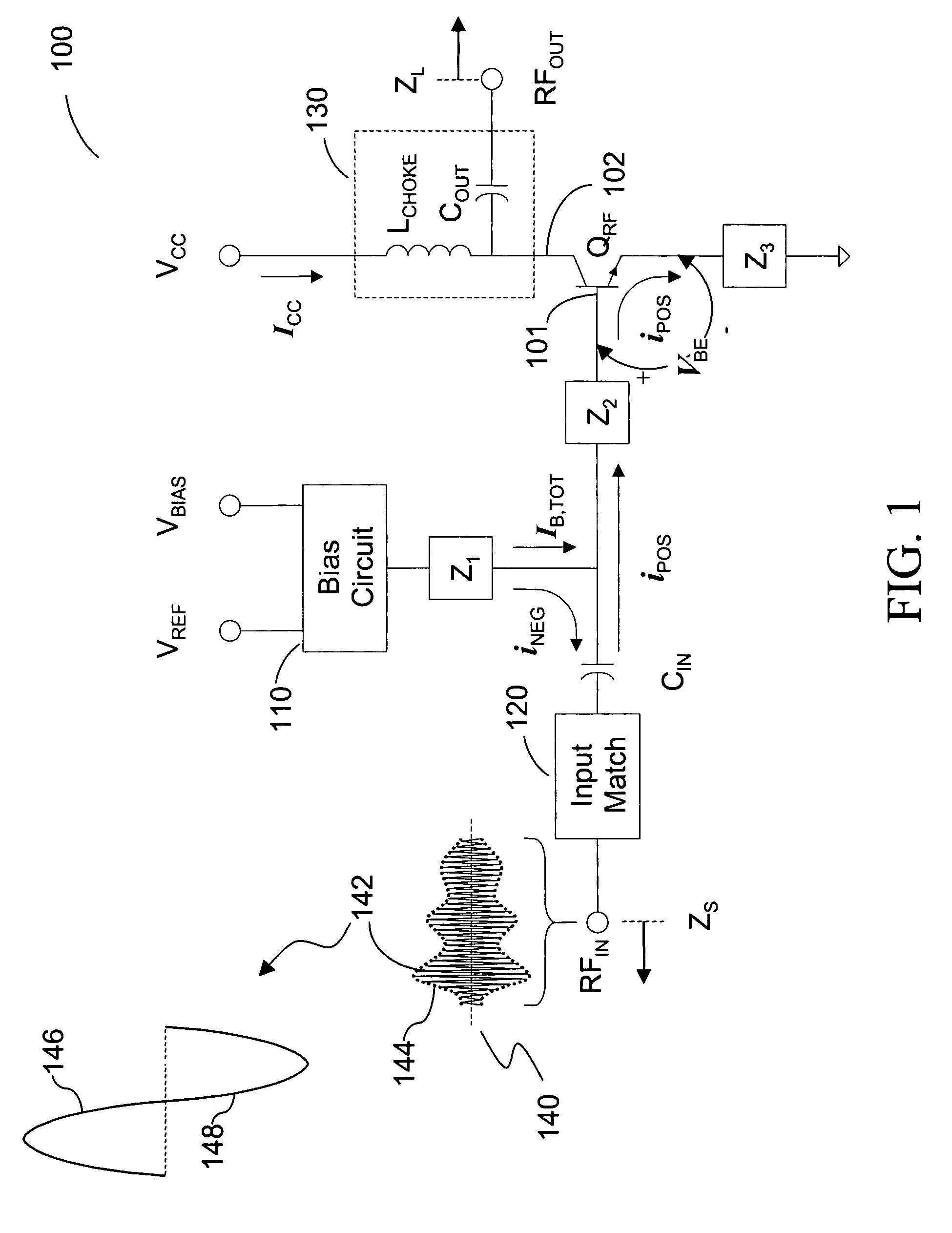
[0023]FIG. 1 depicts a simplified block diagram of a single-stage transistor amplifier network (amplifier) 100, according to one embodiment of the present invention. As shown in FIG. 1, amplifier 100 includes an RF power-amplifying device QRF having an input 101 and an output 102, a bias circuit 110 coupled to the input 101 of the power-amplifying device QRF, an input impedance matching section 120 also coupled to the input 101 of the power-amplifying device QRF through a blocking capacitor CIN, an output bias and impedance matching section 130 coupled to the output 102 of the power-amplifying device QRF, and terminals RFIN, RFOUT, VREF, VBIAS, and VCC.

[0024] Terminal RFIN is coupled to the input impedance match section 120 for receiving an RF input signal, terminal RFOUT is coupled to the output bias and impedance match section 130 for outputting an amplified RF signal, terminal VCC is for connecting to a primary power supply voltage used to power the amplifier network 100 and is ...


PUM


Abstract

The embodiments of the present invention include a bias circuit for a power-amplifying device, which receives and amplifies an input RF signal having a series of RF cycles within a modulation envelop. The bias circuit compensates odd-order distortion processes by detecting the power in the input signal and providing a dynamic adjustment to a bias stimulus for the power-amplifying device within a time scale of the modulation envelope.

Description

FIELD OF THE INVENTION [0001] The present invention relates to radio-frequency (RF) power amplifier circuits and, in particular, to bias circuits that serve to minimize distortion in the amplifier circuits. BACKGROUND OF THE INVENTION [0002] Electronic equipment such as computers, wireless devices, broadband devices, radios, televisions and other similar devices communicate with each another by transmitting signals through air, space and guided media such as wire, cable, microstrip, waveguide, and optical fiber. These transmission signals undergo a variety of processes throughout their communication paths, one of which involves amplifying the signals using power amplifiers. [0003] A radio frequency (RF) power amplifier is a circuit that is capable of receiving an RF input signal and amplifying it to produce an RF output signal that is a magnified version of the input signal. RF power amplifiers are frequently used in communications systems such as wireless telephony, satellite links...

Claims


Application Information

Patent Timeline
IPC IPC(8): H03G3/10
CPCH03F1/30H03F1/32H03F3/191H03F3/605H03F2200/18H03F2200/222H03F2200/391H03F2200/451
Inventor WANG, NANLEI LARRYSTRIFLER, WALTER A.
Owner WJ COMM
Why Eureka
Try Eureka