Thin-film transistor, method of producing thin-film transistor, electronic circuit, display, and electronic device

a thin-film transistor and organic semiconductor technology, applied in transistors, optics, instruments, etc., can solve the problems of insufficient investigation on the optimum layer structure, loss of semiconductor properties, and difficulty in realizing a thin-film transistor using an organic semiconductor layer with high performance and operable with a small driving voltage, etc., to achieve low driving voltage, easy and highly reliable manner, and good transistor characteristics

Inactive Publication Date: 2007-05-03
SEIKO EPSON CORP
View PDF15 Cites 107 Cited by
  • Summary
  • Abstract
  • Description
  • Claims
  • Application Information

AI Technical Summary

Benefits of technology

[0014] An exemplary embodiment of the invention provides a thin-film transistor having good transistor characteristics and capable of operating with a low driving voltage, a method of producing such a thin-film transistor in an easy and highly reliable manner, a high-reliability electronic circuit, a display, and an electronic device.
[0015] In an aspect, the invention can provide a thin-film transistor having an organic semiconductor layer including a channel region, a source region and a drain region formed such that the channel region is disposed between the source region and the drain region, a gate electrode corresponding to the channel region, and a gate insulating layer disposed between the gate electrode and the organic semiconductor layer and having an alignment surface layer on a side facing the organic semiconductor layer, the alignment surface layer serving to align the organic semiconductor layer. The thin-film transistor in this aspect of the invention has good transistor characteristics and can operate with a low driving voltage.
[0016] In this thin-film transistor, the alignment surface layer may be formed by aligning the gate insulating layer in a particular direction, and the organic semiconductor layer may be aligned by the alignment surface in a direction along the particular direction. The alignment surface layer may be formed by forming a plurality of grooves in a particular direction on a surface, facing the organic semiconductor layer, of the gate insulating layer, and the organic semiconductor layer may be aligned in the particular direction by the alignment surface layer. The resultant thin-film transistor produced in this manner has good transistor characteristics and can operate with a low driving voltage.

Problems solved by technology

However, the carrier mobility of the organic semiconductor layer is generally two or more orders of magnitude smaller than that of semiconductor layers formed of an inorganic material such as silicon, and thus it is very difficult to realize a thin-film transistor using an organic semiconductor layer having high performance and operable with a small driving voltage.
However, sufficient investigation has not been performed on the optimum layer structure, and there is room for improvement in the layer structure.
Besides, if the organic semiconductor layer is exposed to a temperature higher than that temperature, it loses properties of semiconductor.
Another problem with the organic semiconductor layer is that it is easily damaged by an etchant such as a sulfuric acid used in photolithography process.
For the above-described reasons, high-temperature film deposition techniques such as plasma CVD or sputtering and photolithography process cannot be used to form the gate insulating film and the gate electrode.
Any material that needs a similar micro fabrication technique cannot be employed.
Thus, when a thin-film transistor is formed using an organic semiconductor layer, a high enough carrier mobility of the organic semiconductor layer is not achieved, and thus a high driving voltage is required, and the operating speed is low.

Method used


Image

  • Thin-film transistor, method of producing thin-film transistor, electronic circuit, display, and electronic device
  • Thin-film transistor, method of producing thin-film transistor, electronic circuit, display, and electronic device
  • Thin-film transistor, method of producing thin-film transistor, electronic circuit, display, and electronic device

Examples


example 1

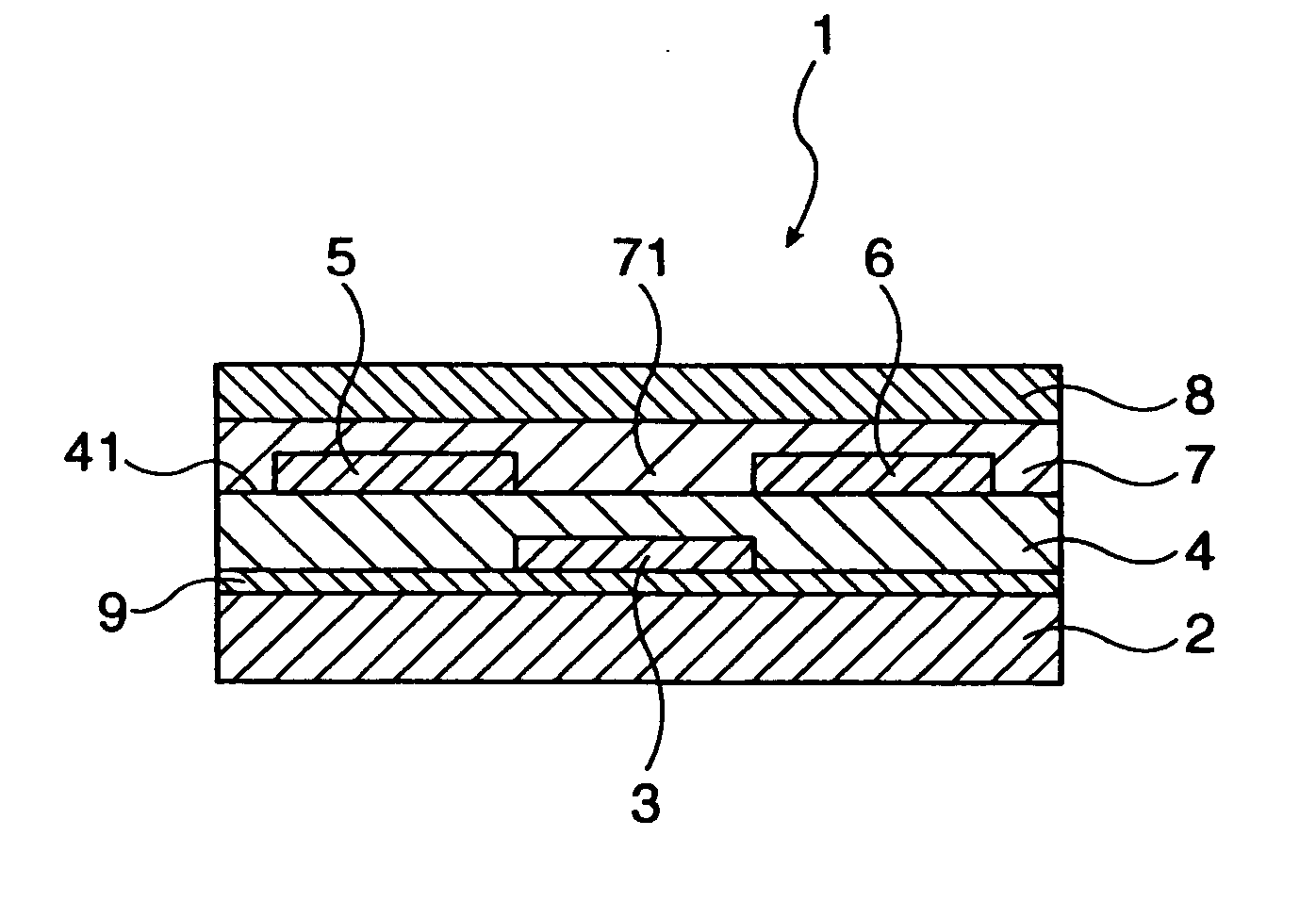
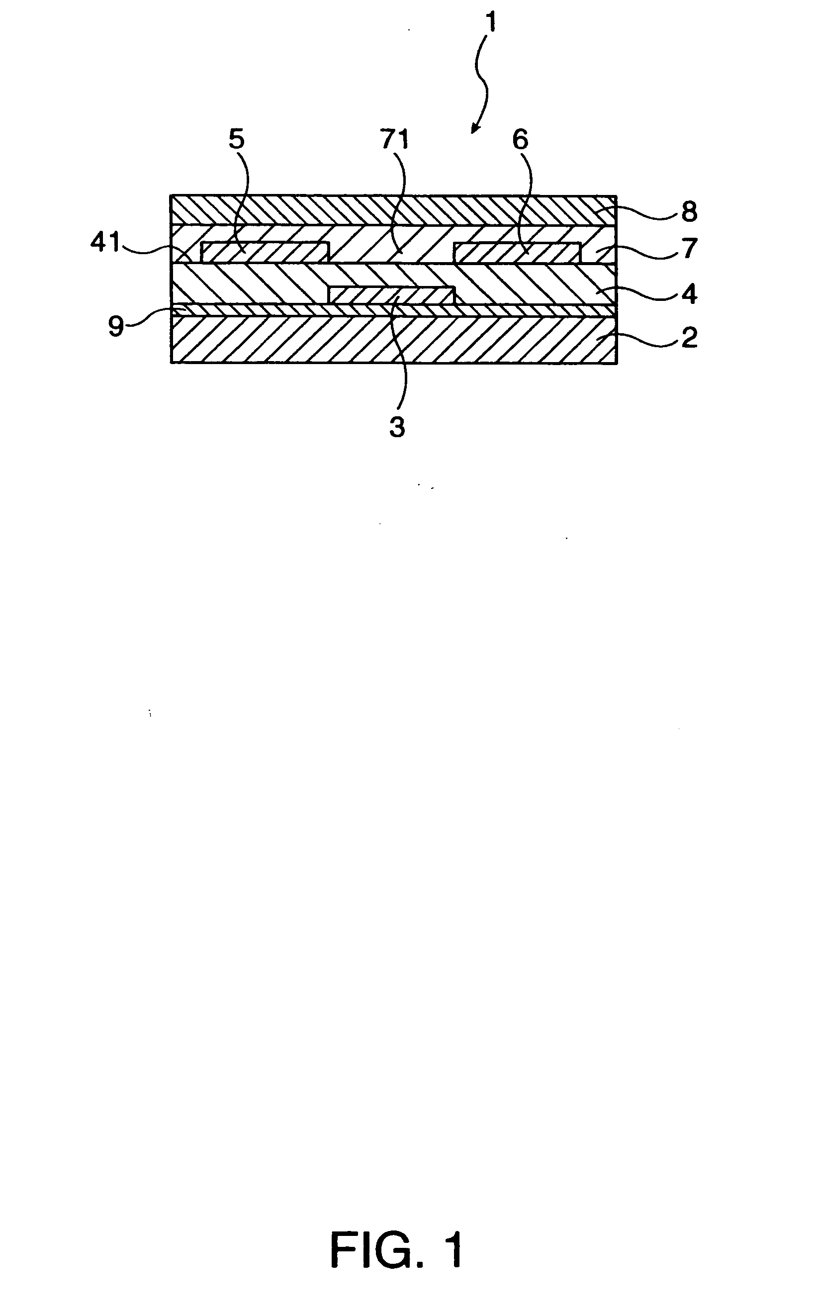
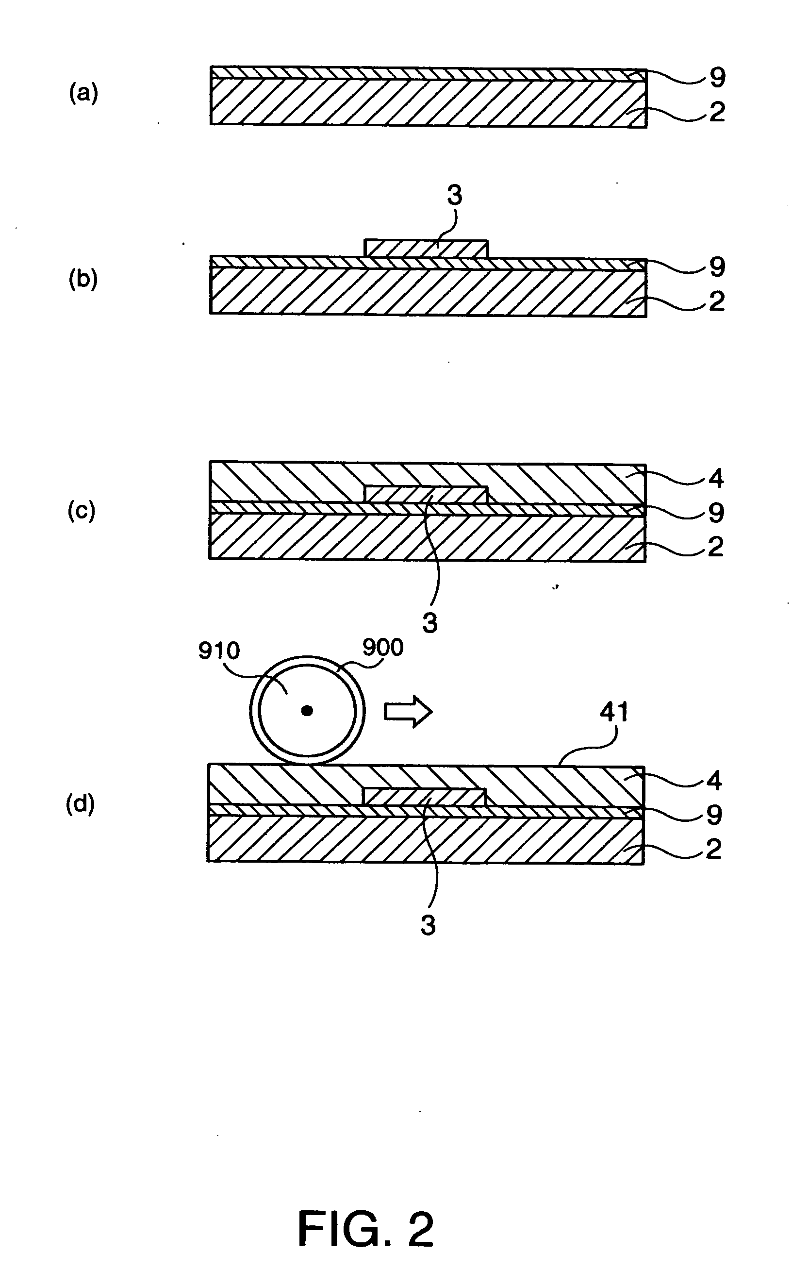
[0179] I-1: First, an underlying layer with an average thickness of 100 nm was formed by depositing SiO2 on a glass substrate by means of CVD process.

[0180] I-2: Thereafter, a Au film with an average thickness of 50 nm was formed on the underlying layer by means of vacuum evaporation, and the Au film was patterned using photolithography process so as to form a gate electrode and an interconnection line extending from the gate electrode.

[0181] I-3: A solution of a precursor of polyimide was coated by means of spin coating on the underlying layer such that the gate electrode was covered. Thereafter, heat treatment was performed at 200° C. for 1 hour thereby forming a gate insulating layer with an average thickness of 200 nm.

[0182] I-4: The upper surface of the gate insulating layer was rubbed using a rubbing apparatus to align the upper surface and a neighboring portion of the gate insulating layer into a predetermined direction. The rubbing conditions were set as follows. The push...

example 2

[0188] II-1: A step similar to step I-1was performed.

[0189] II-2: A step similar to step I-2was performed.

[0190] II-3: A solution of a precursor of polyimide in the form of diallyl ketone was coated by means of spin coating on an underlying layer such that a gate electrode was covered. Thereafter, heat treatment was performed at 200° C. for 1 hour thereby forming a gate insulating layer with an average thickness of 200 nm.

[0191] II-4: Thereafter, a Au film with an average thickness of 50 nm was formed on the gate insulating layer by means of vacuum evaporation, and the Au film was patterned using photolithography process so as to form a source electrode, a drain electrode, and interconnection lines connected respectively with the source electrode and the drain electrode.

[0192] II-5: While heating the gate insulating layer at 180° C., the gate insulating layer was illuminated with polarized light emitted from a polarized light source, thereby aligning the upper surface and a neig...

example 3

[0196] III-1: A step similar to step I-1 was performed.

[0197] III-2: A step similar to step I-2was performed.

[0198] III-3: Thereafter, SiO2 was deposited on an underlying layer by means of CVD process using TEOS (tetraethoxysilane) as a source material such that a gate electrode was covered, thereby forming an inorganic layer with an average thickness of 200 nm. A solution of a precursor of polyimide was coated by means of spin coating on the inorganic layer. Thereafter, heat treatment was performed at 200° C. for 1 hour thereby forming an organic layer with an average thickness of 20 nm.

[0199] III-4: A step similar to step I-4was performed.

[0200] III-5: A step similar to step I-5was performed.

[0201] III-6: A step similar to step I-6was performed.

[0202] III-7: A step similar to step I-7was performed.

[0203] Thus, a thin-film transistor such as that shown in FIG. 6 was obtained.

2. Evaluation

[0204] The carrier mobility in the channel region of the organic semiconductor layer ...


PUM

PropertyMeasurementUnit
temperatureaaaaaaaaaa
thicknessaaaaaaaaaa

Abstract

Aspects of the invention can provide a thin-film transistor having good transistor characteristics and operable with a low driving voltage, a method of producing such a thin-film transistor, a high-reliability electronic circuit, a display, and an electronic device. In an exemplary thin-film transistor according to the invention, a gate electrode can be formed on a substrate via an underlying layer, and a gate insulating layer can be formed on the substrate such that the gate electrode is covered with the gate insulating layer. A source electrode and a drain electrode are formed on the gate insulating layer such that they are separated from each other by a gap formed just above the gate electrode. An organic semiconductor layer can be formed thereon such that the electrodes are covered with the organic semiconductor layer. A region between the electrodes of the organic semiconductor layer functions as a channel region. A protective layer can be arranged on the organic semiconductor layer. This thin-film transistor is characterized in that the organic semiconductor layer is formed after the gate insulating layer is formed, and the gate insulating layer has the capability of causing the organic semiconductor layer to be aligned.

Description

[0001] This is a Divisional of application Ser. No. 10 / 880,572 filed Jul. 1, 2004. The disclosure of the prior application is hereby incorporated by reference herein in its entirety.BACKGROUND OF THE INVENTION [0002] 1. Field of Invention [0003] An aspect of the invention relates to a thin-film transistor, a method of producing a thin-film transistor, an electronic circuit including a thin-film transistor, a display including a thin-film transistor, and an electronic device including a thin-film transistor. [0004] 2. Description of Related Art [0005] In recent years, thin-film transistors using an organic material behaving as a semiconductor in electrical conduction (organic semiconductor material) have been developed. Thin-film transistors of this type have an advantage that a semiconductor layer can be produced by a process using a solution without needing a high-temperature process or a high-vacuum process. The thin-film transistors of this type are also advantageous in that they...

Claims


Application Information

Patent Timeline
Patent Type & Authority Applications(United States)
IPC IPC(8): H01L21/00G02F1/167G02F1/1368H01L21/31H01L21/316H01L21/336H01L29/786H01L51/00H01L51/05H01L51/30H01L51/40
CPCG02F1/1368H01L21/31608H01L51/0012H01L51/0036H01L51/0545H01L51/0039H01L51/0043H01L51/0516H01L51/0037H10K71/191H10K85/1135H10K85/115H10K85/113H10K85/151H10K10/468H10K10/466H10K10/476
Inventor MORIYA, SOICHI
Owner SEIKO EPSON CORP
Why Eureka
Try Eureka