Eureka AIR delivers breakthrough ideas for toughest innovation challenges, trusted by R&D personnel around the world.

Power distribution for high-speed integrated circuits

Active Publication Date: 2007-05-10
ORACLE INT CORP
View PDF26 Cites 10 Cited by
  • Summary
  • Abstract
  • Description
  • Claims
  • Application Information

AI Technical Summary

Problems solved by technology

As frequencies in high speed electronic devices increase, it becomes more challenging to provide effective power supply decoupling.
For the circuit designer, providing high speed devices with adequate current in the time required becomes more challenging as switching speeds increase.
Consequently, too few capacitors are used to provide adequate current to all the power pins or the capacitors are placed too far away from the power pins to effectively provide current to the device.
However, there is a price for achieving higher propagation velocities.
This overlap in decoupling regions results in higher noise levels in the power being provided to each IC.

Method used


Image

  • Power distribution for high-speed integrated circuits
  • Power distribution for high-speed integrated circuits
  • Power distribution for high-speed integrated circuits

Examples


Embodiment Construction

)

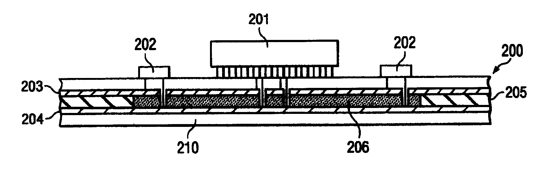
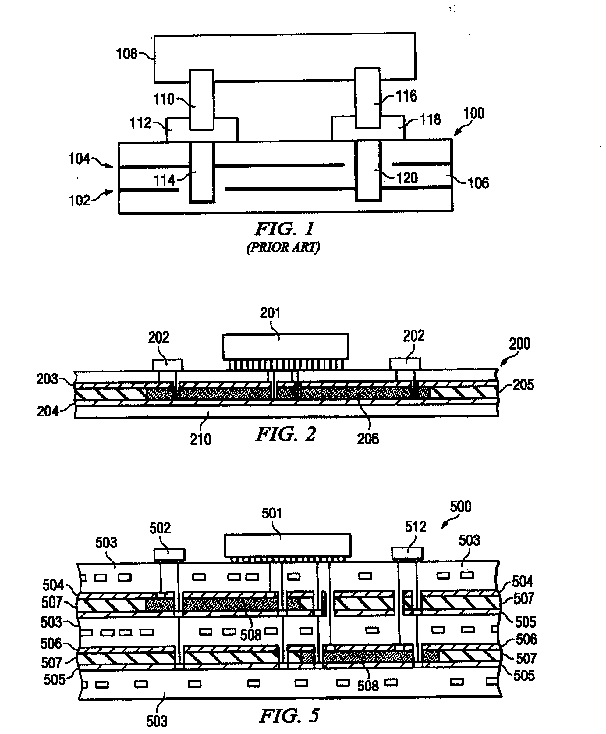
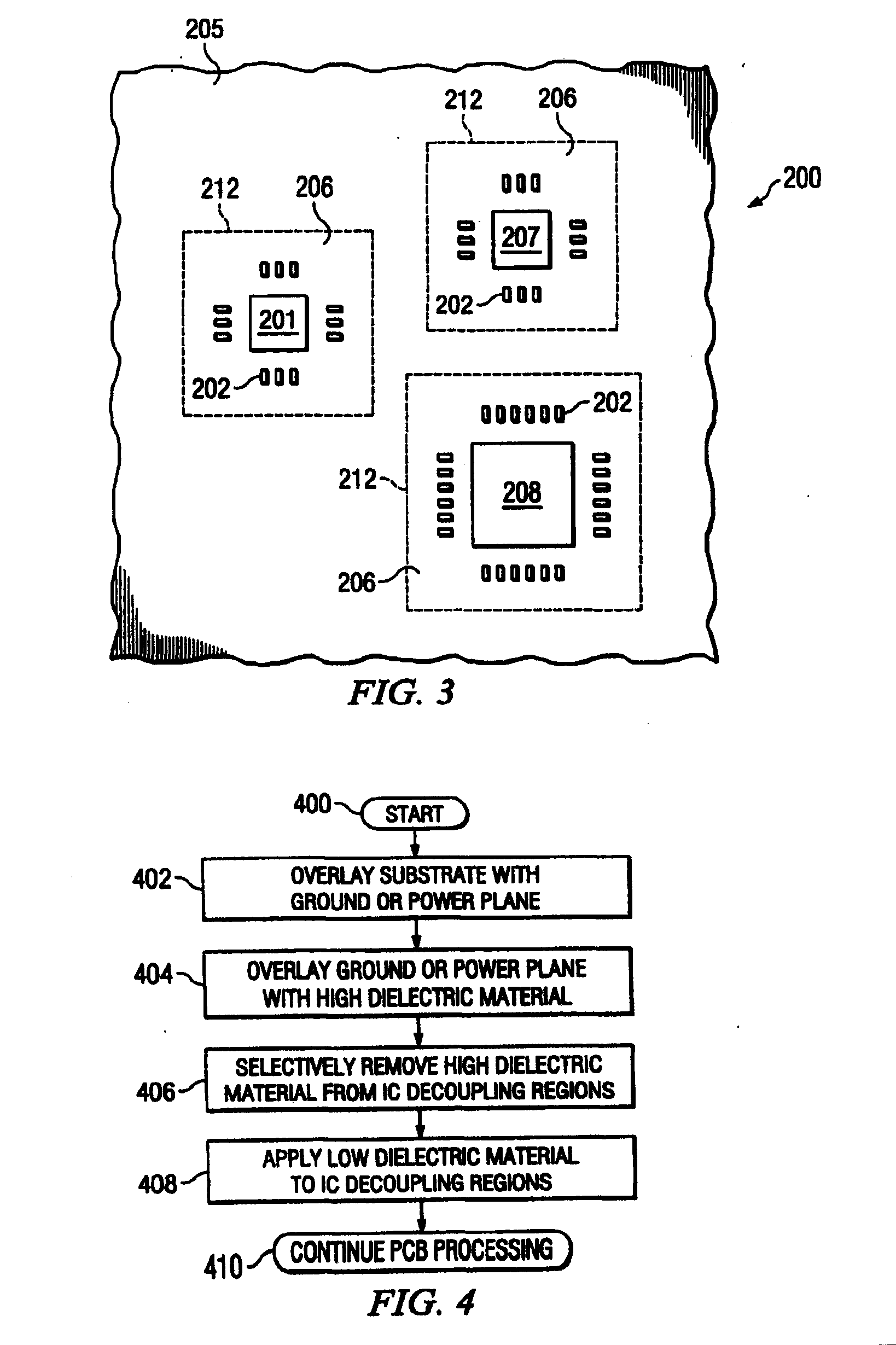
[0017]FIG. 1 shows a typical power-ground plane construction according to the prior art, shown in the context of printed circuit board (PCB) 100 and device 108 (such as an integrated circuit) mounted thereon. In this example, the PCB 100 is composed of two internal planes 102, 104, for example, within a printed circuit board. One plane 102 is a ground plane or layer, while plane 104 is voltage plane or layer. Sandwiched between planes 102 and 104 is a dielectric layer 106. These internal layers create a buried capacitance structure used for decoupling of integrated circuit (IC) device 108 that is attached to printed circuit board 100. In this example, IC device 108 has a connection 110 by way of solder pad 112 and via 114 to power plane 104, and another connection 116 by way of solder pad 118 and via 120 to ground plane 102. In typical prior art structures, ground and power planes 102, 104 are formed of a conductor material such as copper, and dielectric layer 106 is composed of a ...


PUM


Abstract

An improved technique for power distribution for use by high speed integrated circuit devices. A mixture of high dielectric constant, Er and low Er materials are used in a dielectric layer sandwiched between the voltage and ground planes of a printed circuit board that is used to fixture one or more integrated circuit devices. The low Er material is used in an area contained by the location of the integrated circuit device and its corresponding decoupling capacitors located nearby. High Er material is used in areas between the regions of low Er material. The low Er material improves that speed at which current from an adjoining decoupling capacitor can propagate to a power pin of the integrated circuit device. The high Er material mitigates cross-coupling of noise between the low Er regions.

Description

CROSS-REFERENCE TO RELATED APPLICATIONS [0001] This application is a continuation-in-part of U.S. application Ser. No. 11 / 269,348 filed Nov. 5, 2005, the disclosure of which is hereby incorporated in its entirety.BACKGROUND OF THE INVENTION [0002] 1. Field of the Invention [0003] The present invention relates generally to techniques for improving power distribution for electrical and electronic devices, and more particularly relates to techniques for distributing power for use by high speed integrated circuit devices. [0004] 2. Background Art [0005] As frequencies in high speed electronic devices increase, it becomes more challenging to provide effective power supply decoupling. Integrated circuit devices (ICs) require high frequency current for their operation. The current requirements for such IC devices must be identified to properly assess the decoupling and power distribution requirements. [0006] High speed ICs are typically mounted on printed circuit boards (PCBs). Sufficient ...

Claims


Application Information

Patent Timeline
IPC IPC(8): H01L23/04
CPCH01L23/49822H01L2224/16H05K1/0231H05K1/024H05K2201/0187H05K2201/09309H05K2201/10734H01L2924/01019H01L2924/01068
Inventor HORN, KEVINDILLINGER, FORESTBUHLER, OTTO RICHARDSAUTER, KARL
Owner ORACLE INT CORP
Why Eureka
Eureka Blog
Learn More