Differential critical dimension and overlay metrology apparatus and measurement method

Inactive Publication Date: 2007-05-10
IBM CORP
View PDF46 Cites 112 Cited by
  • Summary
  • Abstract
  • Description
  • Claims
  • Application Information

AI Technical Summary

Benefits of technology

[0023] Preferably, variations in intensities of the first non-zero diffracted order is collected, although the invention contemplates that any, or multiple, detectable non-zero diffracted order may be used. Through the use of multi-wavelength or broadband illumination, the method allows for the measurement and control o

Problems solved by technology

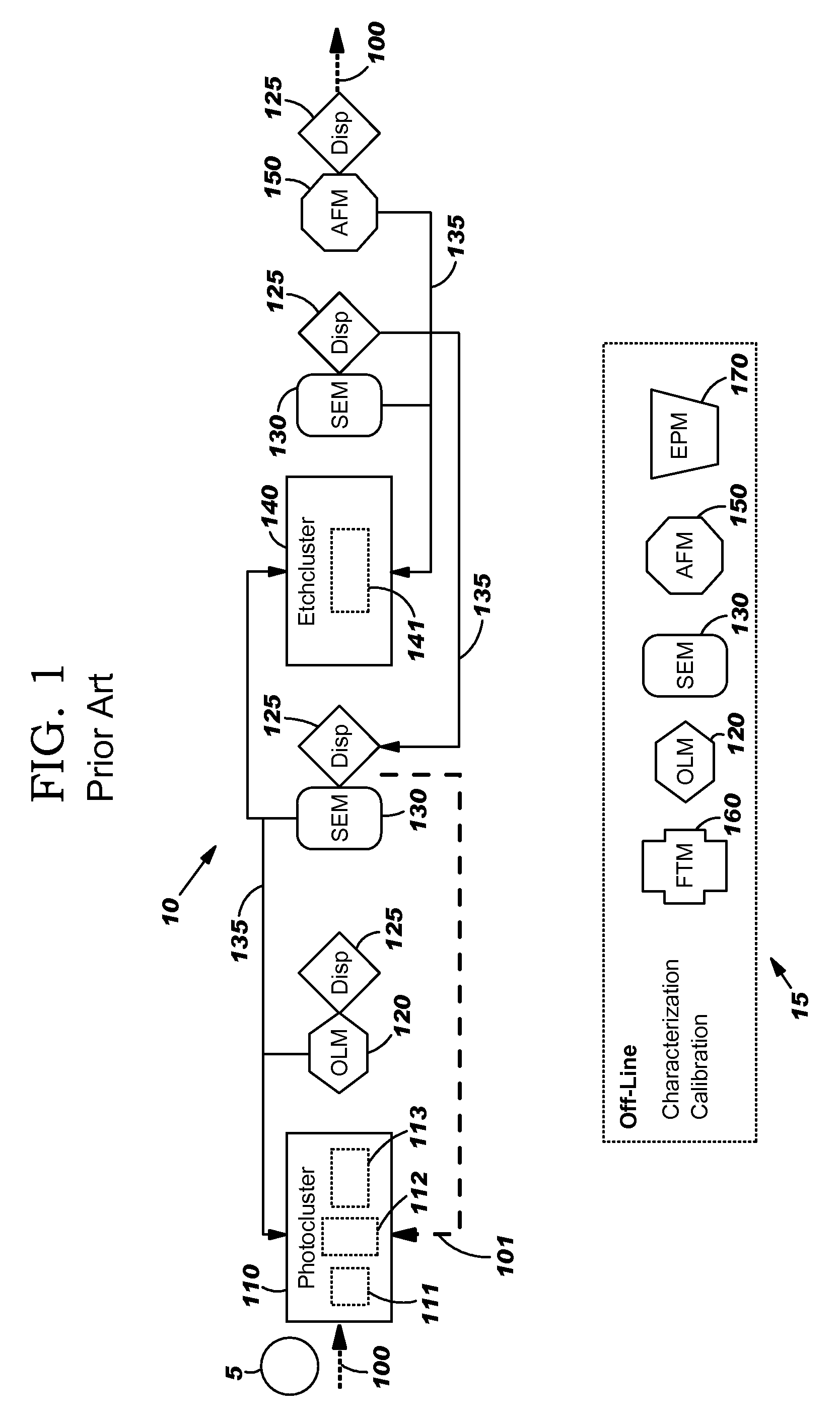
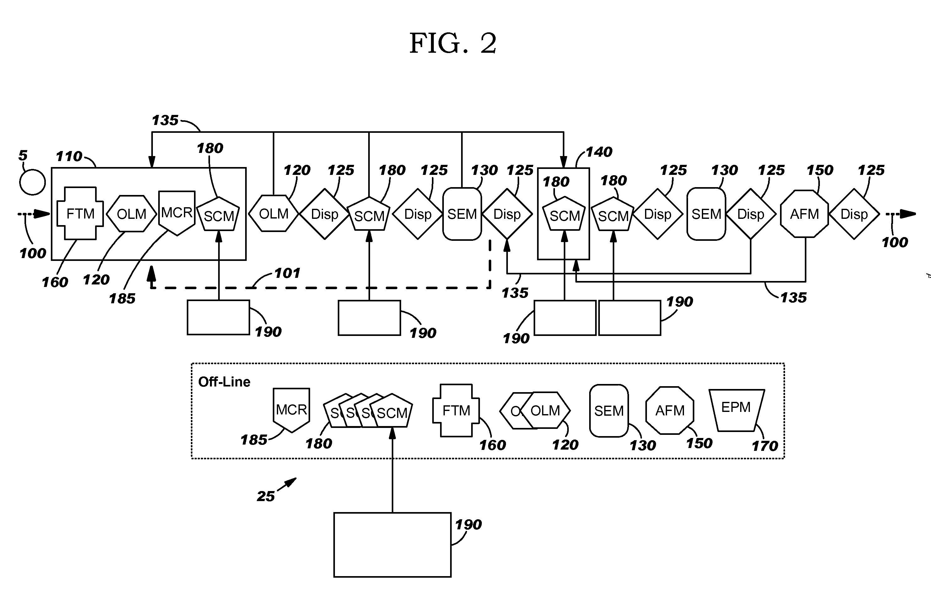
Although such a hypothetical processing system 20 would have increased metrology capability over conventional systems, this increased capability would come at the expense of increased complexity and cost.
Those libraries are costly and time-consuming to develop, and also require computer servers 190 and associated databases to perform the required comparisons.
However, scatterometry is computationally intensive, and requires server farms and databases containing signal libraries, thus increasing complexity and cost.
Since conventional scatterometry is not a differential measurement, its application to CD measurement is susceptible to noise: for example, measurement variation such as illumination, wavelength, detector response, target alignment; process variation such as film thicknesses and optical properties.
Conventional scatterometry is also restricted to detection of the zeroth diffracted order, which can be used to characterize film thickness, but has typically poor signal to

Method used


Image

  • Differential critical dimension and overlay metrology apparatus and measurement method
  • Differential critical dimension and overlay metrology apparatus and measurement method
  • Differential critical dimension and overlay metrology apparatus and measurement method

Examples


embodiment 1701

[0124] A preferred embodiment 1701 of the inventive discrete differential grating target 455 for use in measuring CD is shown in FIG. 17. This exemplary target 1701 provides a preferred means of CD measurement that places no restriction on the nominal CD size. The target grating 1701 is divided into two or more sub-pattern regions, e.g. Region 1 (reference numeral 1731) and Region 2 (reference numeral 1732), comprised of lines, e.g. 1711, 1712, respectively, having length H oriented along the y-direction. The nominal widths, e.g. Wd1, Wd2, of lines 1711, 1712, respectively, are uniform within each sub-pattern region 1731, 1732, respectively, but are different between sub-pattern regions 1731, 1732, respectively (e.g. first sub-pattern region 1731 including lines 1711 having nominal width Wd1, and second sub-pattern region 1732 having lines 1712 of nominal width Wd2). The features 1711, 1712 are preferably joined by connecting regions 1750, which can help avoid line shortening of the...

embodiment 3000

[0134] Another target embodiment 3000, shown in FIG. 30, enables the application of the inventive differential diffractometry measurement to the parallel acquisition of through-pitch CD measurements. The measured dependence of the printed CD on pitch or period is critical to the determination of the Optical Proximity Correction (OPC) rules. OPC rules govern the modification of product mask layouts to ensure simultaneous printing of differently pitched features to a common size. A current limitation of OPC rules generation is that the conventional SEM CD measurement approach is slow and laborious. In particular, SEM CD measurement precludes the gathering of sufficient data to ensure the matching of the printed CDs over a representative process window. The target of FIG. 30 is comprised of multiple differential gratings 3001, 3002, 3003, 3004, each similar in design to that shown in FIG. 17 where the period, Pa, Pb, Pc, Pd, respectively, is changed from one differential grating to the...


PUM


Abstract

A method is described for measuring a dimension on a substrate, wherein a target pattern is provided with a nominal characteristic dimension that repeats at a primary pitch of period P, and has a pre-determined variation orthogonal to the primary direction. The target pattern formed on the substrate is then illuminated so that at least one non-zero diffracted order is detected. The response of the non-zero diffracted order to variation in the printed characteristic dimension relative to nominal is used to determine the dimension of interest, such as critical dimension or overlay, on the substrate. An apparatus for performing the method of the present invention includes an illumination source, a detector for detecting a non-zero diffracted order, and means for positioning the source relative to the target so that one or more non-zero diffracted orders from the target are detected at the detector.

Description

TECHNICAL FIELD [0001] The present invention relates generally to semiconductor manufacturing and, more particularly, to monitoring and control of lithographic and etch process conditions used in microelectronics manufacturing. BACKGROUND OF THE INVENTION [0002] During microelectronics manufacturing, a semiconductor wafer is processed through a series of tools that perform lithographic processing, followed by etch processing, to form features and devices in the substrate of the wafer. Such processing has a broad range of industrial applications, including the manufacture of semiconductors, flat-panel displays, micromachines, and disk heads. [0003] The lithographic process allows for a mask or reticle pattern to be transferred via spatially modulated light (the aerial image) to a photoresist (hereinafter, also referred to interchangeably as resist) film on a substrate. Those segments of the absorbed aerial image, whose energy (so-called actinic energy) exceeds a threshold energy of c...

Claims


Application Information

Patent Timeline
IPC IPC(8): G03B27/00G03C5/00G03B27/42B81C99/00G01B9/00G03F7/20G03F9/00
CPCB81C99/0065G03F7/70608G03F7/70625G03F7/70633G03F7/70691
Inventor AUSSCHNITT, CHRISTOPHER
Owner IBM CORP
Why Eureka
Try Eureka