Automated process and apparatus for planarization of topographical surfaces
a topographical surface and automatic process technology, applied in the direction of electrical apparatus, coatings, basic electric elements, etc., can solve the problems of affecting the final yield or performance of the device, the non-planar surface is no longer suitable for constructing the next structural layer, and the non-planar surface cannot be replanarized. achieve the effect of high planarization ratio and quick and efficient planarization of various coated substrates
- Summary
- Abstract
- Description
- Claims
- Application Information
AI Technical Summary
Benefits of technology
Problems solved by technology
Method used
Image
Examples
example i
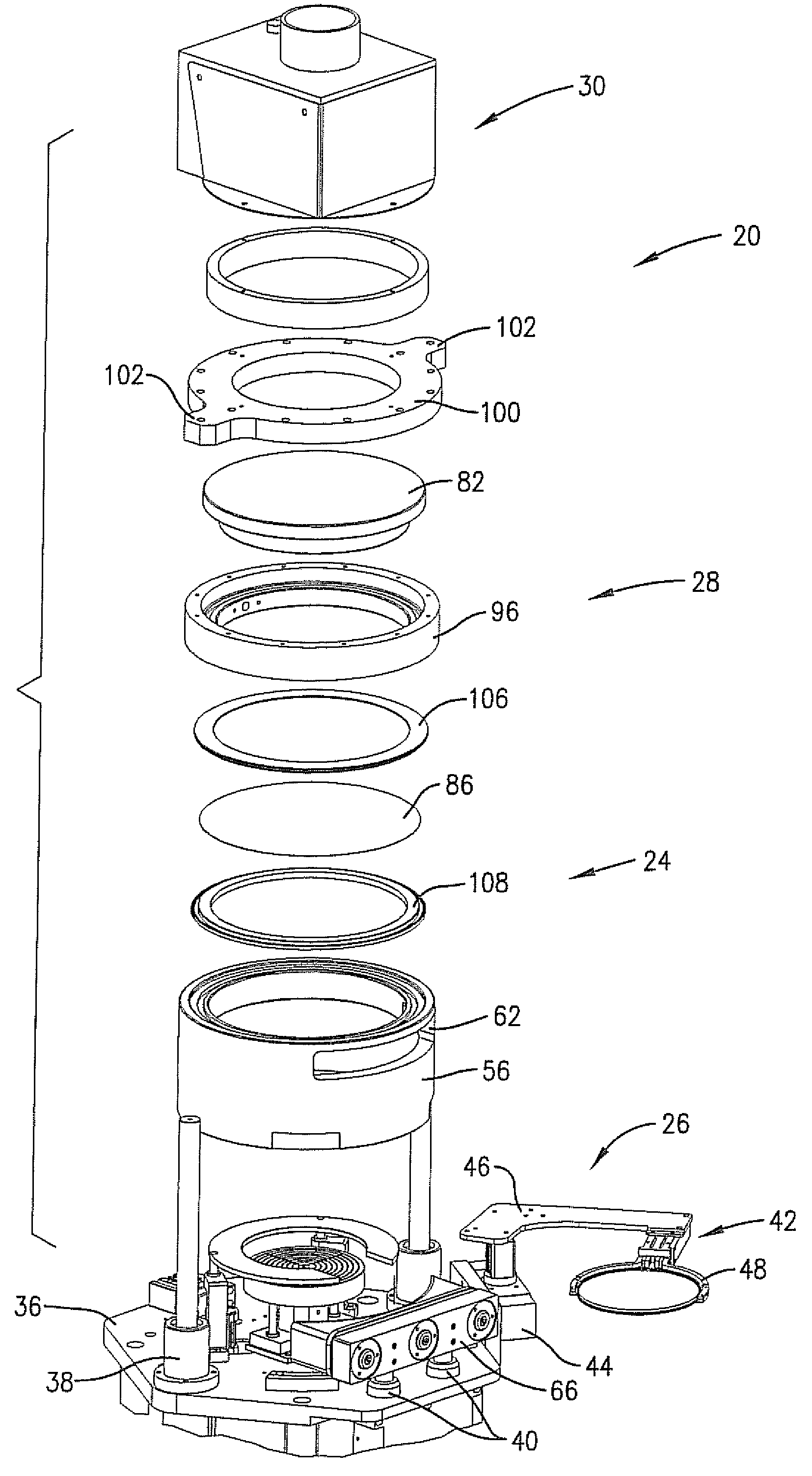
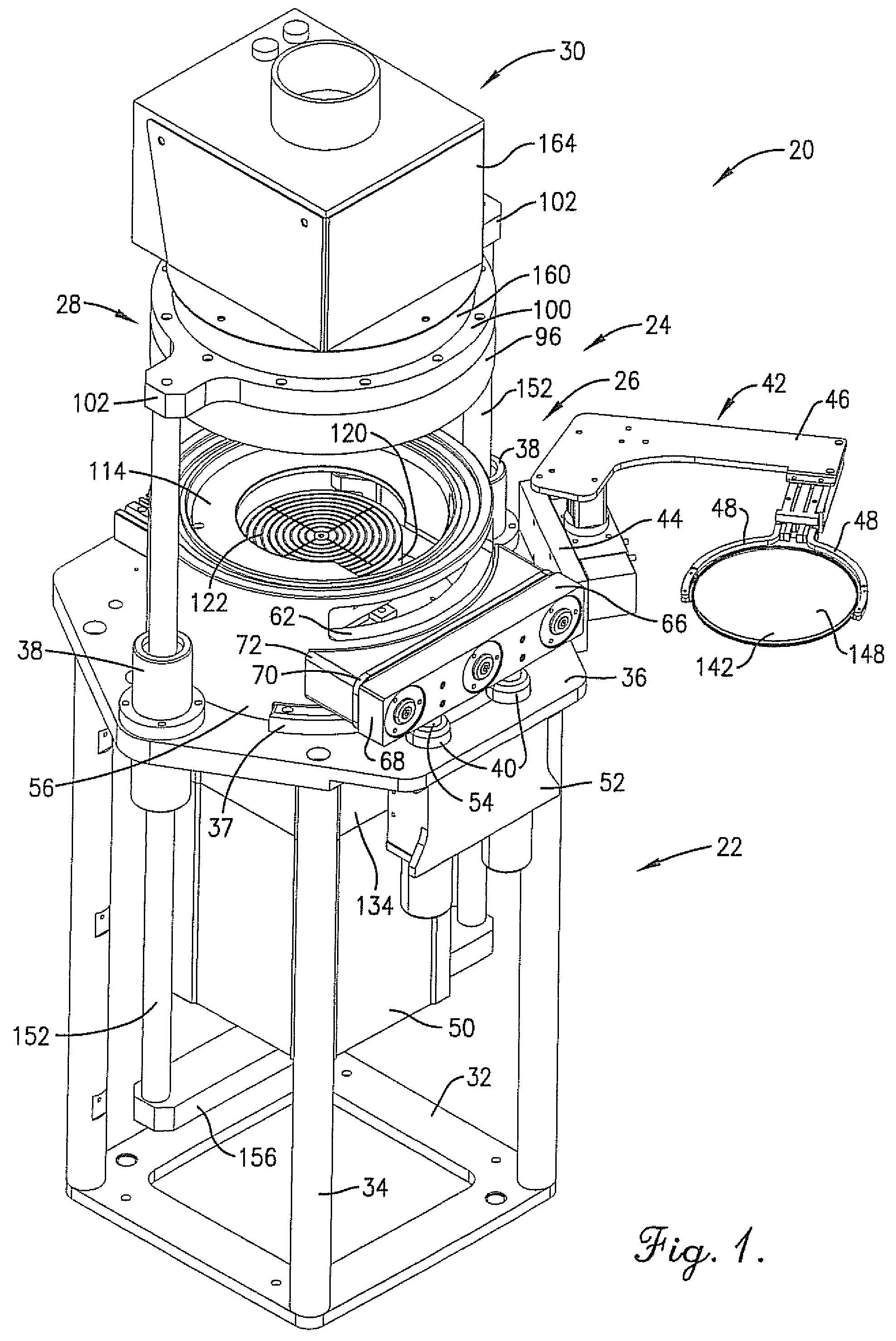
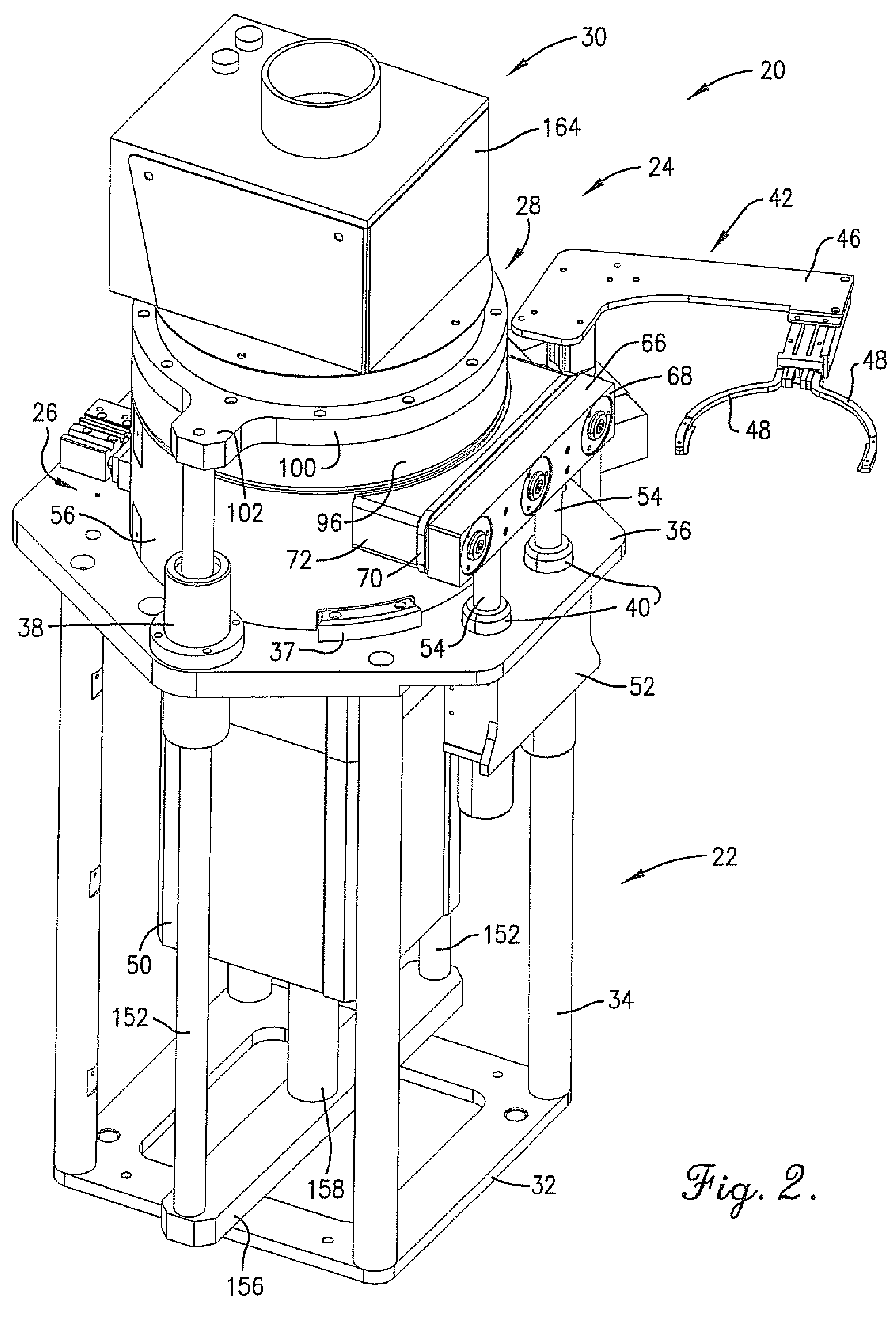
[0062] In this example, a trench wafer having a photocurable material was planarized using apparatus 20. In particular, a silicon wafer having trench structures about 1 μm was used as the substrate. The featured density of the wafer ranged from about 4-96%. A photocurable material was prepared by thoroughly mixing 20 grams of epoxy (D.E.R. 354LV, Dow Chemical Co.), 80 grams of propylene glycol monomethyl ether (PGME, Aldrich Chemical Co.), and 1.2 grams of Sarcat KI-85 (Sartomer Chemical) in a yellow-lighted laboratory. The material was then filtered using a 0.2 μm filter and stored in a clean brown bottle. A film of the photocurable planarization material less than 0.5 μm thickness was spin-coated onto the silicon trench wafer.
[0063] During processing, the closed apparatus chamber was evacuated to less than 20 torr for about 30 seconds to remove residual solvent. During planarization, the substrate was pressed against the Teflon optical flat surface using a force of about 68 psi f...
example ii
[0065] In this example a thermocurable material was applied to a silicon wafer. The wafer was prepared by first coating it with a silicon dioxide film having a thickness of about 1 μm. A pattern containing vias of 0.2 to 1 μm in diameter and having various feature density areas was patterned into the silicon dioxide film. The depth of the vias was about 1 μm. A thermocurable material was prepared as set forth in Example I, except that 1.0 grams of Nacure® Super XC-A 230 catalyst (King Industries) was used in lieu of the Sarcat product. The material was spin-coated to a thickness of about 0.2 μm onto the silicon via wafer.
[0066] The coated wafer was transferred to the apparatus 20 which, after sealing, was evacuated to less than about 20 torr for about 180 seconds to remove residual solvent. The coated substrate was pressed against the optical flat surface using a force of 68 psi for 60 seconds. During this time a pulsing UV / infrared heating light was illuminated through the optical...
example iii
[0068] In this example, photocurable planarization material consisting of 5 grams of Novolac epoxy resin (D.E.R.™ 354LV, The Dow Chemical Company), 5 grams oft-butyl glycidyl ether (Aldrich), and 0.6 grams of 500% triarylsulfonium hexafluorophosphate (a photo acid generator) solution (Aldrich) was formulated and mixed thoroughly. The solvent used in the photo acid generator solution was a reactive solvent. The material was filtered with 0.2 μm filter.
[0069] A 1.7 μm thick layer of the planarization material was coated onto a 6-inch silicon wafer surface that had been treated with an adhesion promoter APX-K1 (Brewer Science, Inc.) using the vendor's recommended process. A standard edge bead removal process was conducted that removed about 5 mm of edge bead.
[0070] The substrate was placed within the apparatus 20 as described in previous examples, and pressed against the optical flat surface using a pressure of 68 psi for 30 seconds. During this contact, a continuous UV light from a ...
PUM
| Property | Measurement | Unit |
|---|---|---|
| pressure | aaaaa | aaaaa |
| pressure | aaaaa | aaaaa |
| thickness | aaaaa | aaaaa |
Abstract
Description
Claims
Application Information


