
Micro-electronic package structure and method for fabricating the same
a technology of micro-electronic and package structure, which is applied in the direction of semiconductor/solid-state device manufacturing, electric devices, solid-state devices, etc., can solve the problems of contact pads, reduced width of circuits and the reduced size of stencil cavities, so as to reduce the overall thickness of the package structure, simplify the overall fabrication process, and improve flexibility
- Summary
- Abstract
- Description
- Claims
- Application Information
AI Technical Summary
Benefits of technology
Problems solved by technology
Method used
Image

Examples
Embodiment Construction
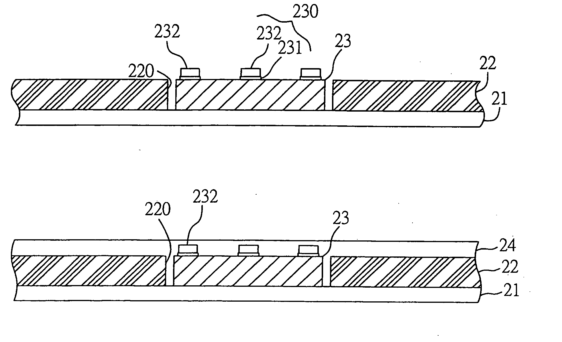
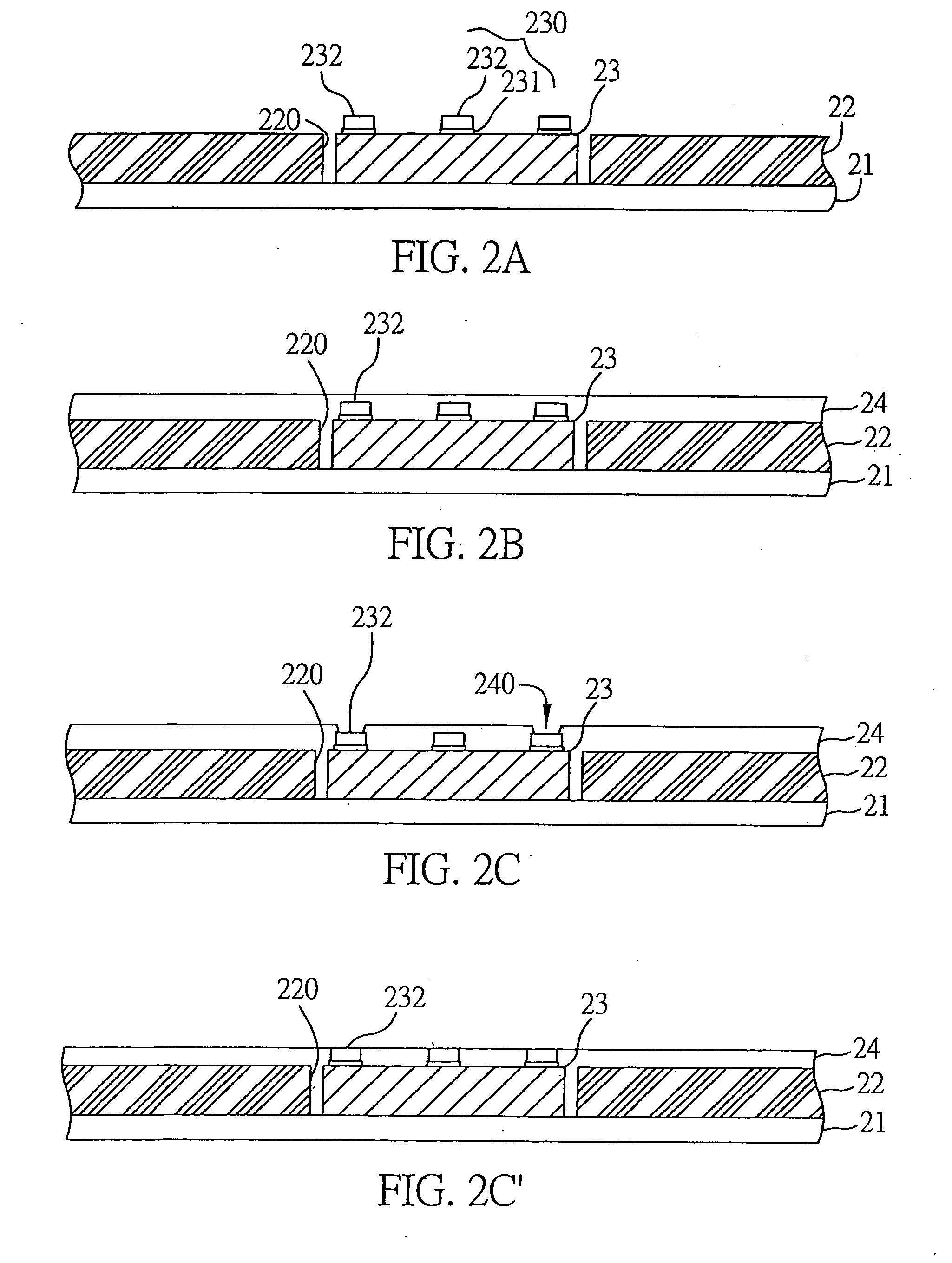
[0025]FIGS. 2A to 2F show the procedural steps of a method for fabricating a micro-electronic package structure in accordance with the present invention.
[0026] Referring to FIG. 2A, a carrier 22 is provided, which can be a metal board, insulating board, or circuit board. The carrier 22 is formed with at least one cavity 220 therethrough. A supporting member 21 may be attached on one side of the carrier 22 and covers one end of the cavity 220. This supporting member 21 can be an adhesive layer or a metal layer, which allows at least one semiconductor chip 23 to be mounted the supporting member 21 and received in the cavity 220 of the carrier 22, wherein electrical connection contacts 230 formed on an active surface of the chip 23 are exposed to the cavity 220. The electrical connection contacts 230 of the chip 23 comprise electrode pads 231 and conductive bumps 232 formed on the electrode pads 231, and are used to establish good external electrical connection for the chip 23.
[0027]...
PUM
 Abstract
Description
Claims
Application Information