

Alloys for flip chip interconnects and bumps
a flip chip and interconnecting technology, applied in semiconductor devices, semiconductor/solid-state device details, electrical apparatus, etc., can solve the problems of increasing the number of i/o connections, increasing the complexity of electronic devices, and suffering from high cost, so as to improve the tarnish resistance of pure silver
Inactive Publication Date: 2007-05-24
WILLIAMS ADVANCED MATERIALS
View PDF10 Cites 38 Cited by
- Summary
- Abstract
- Description
- Claims
- Application Information
AI Technical Summary
Benefits of technology
[0010] The present invention is directed to silver, copper and gold alloys useful for forming UBM and electroplated metal bumps (e.g. bump and / or UBM alloys of silver and gold, silver and palladium, silver, gold and palladium, copper and gold, gold and nickel, gold and palladium, and gold, nickel, and palladium). Silver alloyed with gold improves the tarnish resistance of pure silver while still maintaining a soft and compliant alloy suitable for thermo-sonic bonding to gold plated circuitry. While certain of the herein described silver alloys contain gold, the cost of silver is significantly less than the cost of gold, and the silver alloys of this invention are typically less than 80% of the metal cost of pure gold.
[0011] In another aspect of this invention, copper is alloyed with gold. This combination is quite corrosion resistant, compatible will all materials in these flip chip devices and markedly less expensive. The invention is further directed to the use of gold and silver alloys in the UBM sputtered metal layers and the electroplated bump metals. Other aspects of the invention are directed to semiconductor devices with various bump and / or UBM alloys of silver and gold, silver and palladium, silver, gold and palladium, copper and gold, gold and nickel, gold and palladium, and gold, nickel, and palladium.
[0012] Accordingly, the general object of the invention is to provide bumps and UBM seed layers, and semiconductor devices having such bumps and UBM seed layers, with improved alloy compositions. Another object is to provide bumps and UBM's with alloy compositions which are less expensive than pure gold. Yet another object is to provide alloy compositions for bumps and UBM seed layers which are sufficiently corrosion and / or tarnish resistant. Still another object is to provide bumps and UBM's with alloy compositions with properties which simulate the electrical and / or corrosion resistant properties of gold.
Problems solved by technology
As electronic devices continue to become more complex and smaller, these semiconductors require more I / O connections and the bumps must get closer together than solder bump methods allow.
While gold performs excellently it suffers from very high cost.
Aluminum has system compatibility, but it cannot be made into tall and narrow structures that form the bumps of the flip chip device.
Copper and silver, like gold, have excellent sputtering and electroplating characteristics, but their corrosion resistance is inadequate for them to be reliably bonded onto gold plated circuitry.
Method used
View moreImage
Smart ImageViewing Examples

Examples
example 1
[0029] A silver based alloy comprising about 10% gold.
example 2
[0030] A silver based alloy comprising about 65% gold.
example 3
[0031] A gold based alloy comprising about 30% nickel.
Login to View More PUM
 Abstract
The present invention provides alloys for forming sputtered under bump metallization seed layers and electroplated or otherwise deposited bump metallurgy. The alloys of the present invention are comprised of silver with gold or palladium, copper with gold, or gold with nickel or palladium which provide suitable sputtering and electrical characteristics and resistance to corrosion and tarnishing. The invention further provides for semiconductor devices made from metal alloys for UBM and bump metallurgy, and for a method of making such semiconductor devices.
Description
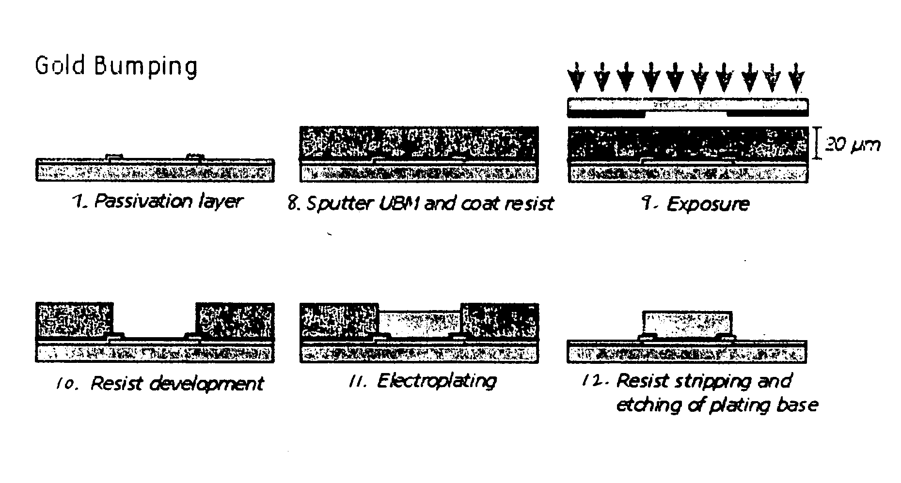
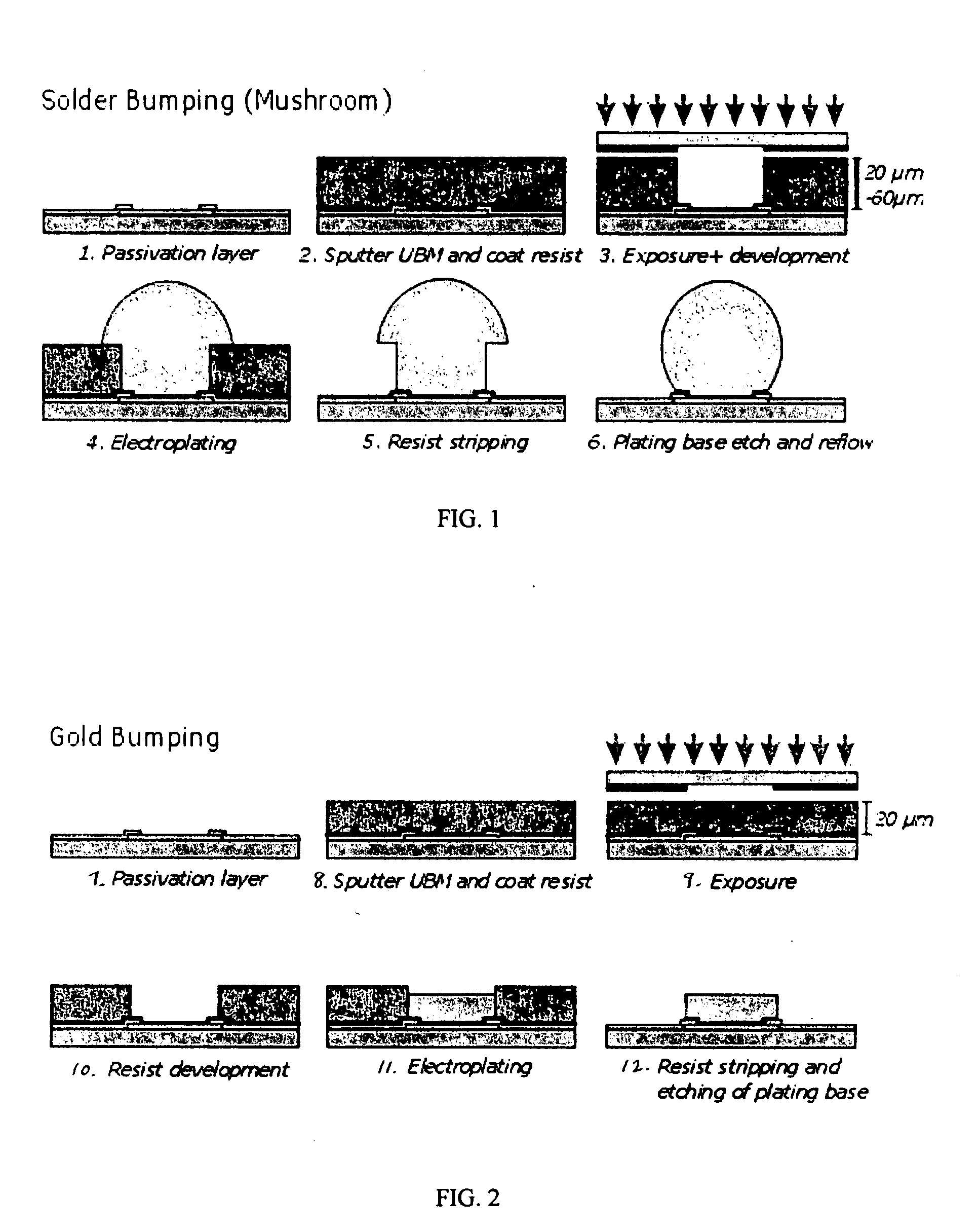
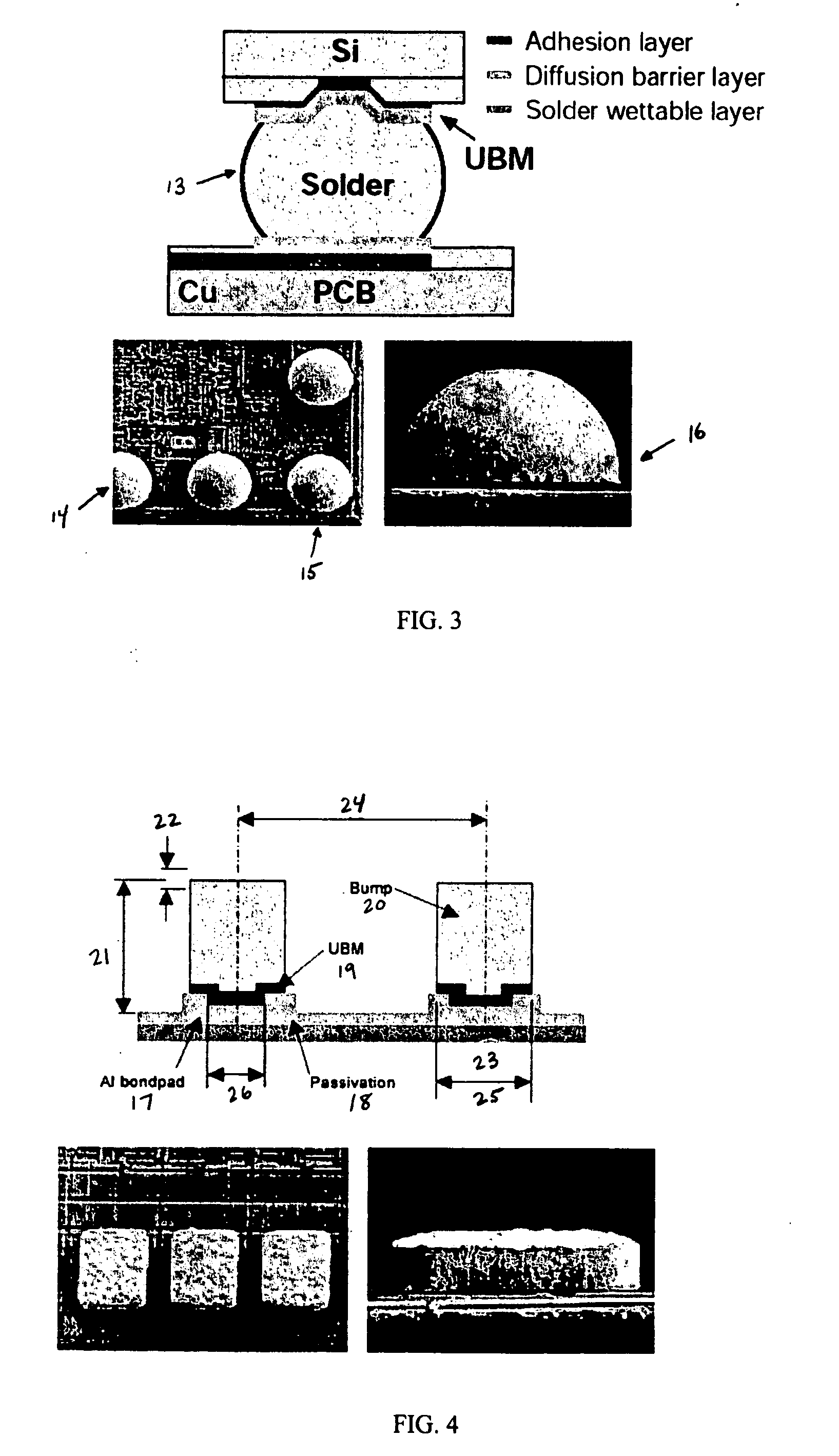
PRIORITY CLAIM [0001] The present application claims priority to Provisional Patent Application No. 60 / 739,584, filed Nov. 23, 2005.TECHNICAL FIELD [0002] The present invention relates to flip chip semiconductor devices and, more particularly, to the materials in the metal bumps of flip chip devices, especially alloys of silver, copper and / or gold metals. BACKGROUND OF THE INVENTION [0003] Currently, gold posts are electroplated onto aluminum, copper or gold electrical junctions on semiconductor devices employing an under bump metallization (UBM) which acts as a diffusion barrier between the semiconductor input / output (I / O) and the bump metallurgy, protects the I / O layer from the atmosphere and acts as a seed layer for an electroplated metal that comprises the bump. Flip chip devices have been marketed for many years and are basically found in two forms. The most common form employs an aluminum semiconductor contact that is sputter coated with chromium or titanium as an adhesion lay...
Claims
Login to View More Application Information
Patent Timeline
 IPC IPC(8): H01L23/48
CPCH01L24/02H01L24/11H01L24/81H01L2224/0401H01L2224/1147H01L2224/13099H01L2224/13139H01L2224/13144H01L2224/13147H01L2224/16H01L2224/8121H01L2224/81815H01L2924/01013H01L2924/01022H01L2924/01028H01L2924/01029H01L2924/01046H01L2924/01047H01L2924/01074H01L2924/01079H01L2924/01082H01L2924/014H01L2924/09701H01L24/13H01L2924/01006H01L2924/01024H01L2924/01033H01L2924/01045
InventorBROWN, DERRICK L.LICHTENBERGER, HEINER
OwnerWILLIAMS ADVANCED MATERIALS