Method for manufacturing non-volatile memory

a non-volatile memory and manufacturing method technology, applied in the direction of basic electric elements, electrical apparatus, semiconductor devices, etc., can solve the problems of affecting the reliability of the device, the electric charge injected into the charge-trapping layer cannot be evenly distributed over the entire charge-trapping layer, and the conventional non-volatile memory cannot integrate with the typical complementary metal-oxide-semiconductor (cmos) circuit process at the same time, so as to achieve effective promotion of device reliability

Inactive Publication Date: 2007-06-07
PROMOS TECH INC
View PDF9 Cites 11 Cited by
  • Summary
  • Abstract
  • Description
  • Claims
  • Application Information

AI Technical Summary

Benefits of technology

[0009] Accordingly, at least one objective of the present invention is to provide a method for manufacturing a non-volatile memory such that the possibility of current leakage problem may be substantially reduced and the reliability of the device can be effectively promoted.

Problems solved by technology

However, if the tunneling oxide layer underneath the polysilicon floating gate has some defects, the defects will provide a pathway for the stored electrical charges to leak away, thereby affecting the reliability of the device.
Obviously, aside from having a leakage current problem, the conventional non-volatile memory can hardly integrate with a typical complementary metal-oxide-semiconductor (CMOS) circuit process at the same time.
Due to the charge-trapping property of silicon nitride, the electric charges injected into the charge-trapping layer will not be evenly distributed over the entire charge-trapping layer.
As a result, aforesaid charge-trapping layer still has difficulties restraining the outflow of current.
In other words, the device leakage problem is only partially resolved.
However, due to coulomb blockade, aforesaid nanocluster can only store a single electric charge at a time.

Method used


Image

  • Method for manufacturing non-volatile memory
  • Method for manufacturing non-volatile memory
  • Method for manufacturing non-volatile memory

Examples


Embodiment Construction

[0031] Reference will now be made in detail to the present preferred embodiments of the invention, examples of which are illustrated in the accompanying drawings. Wherever possible, the same reference numbers are used in the drawings and the description to refer to the same or like parts.

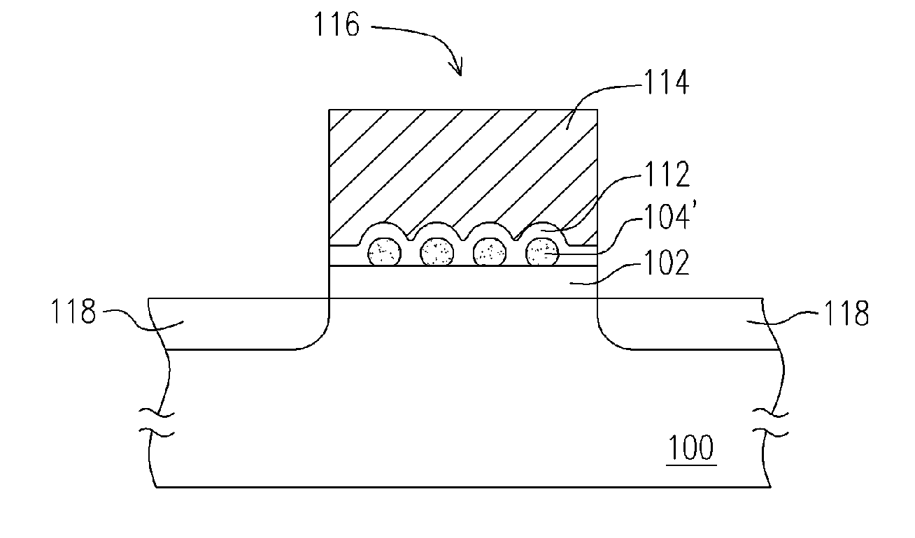
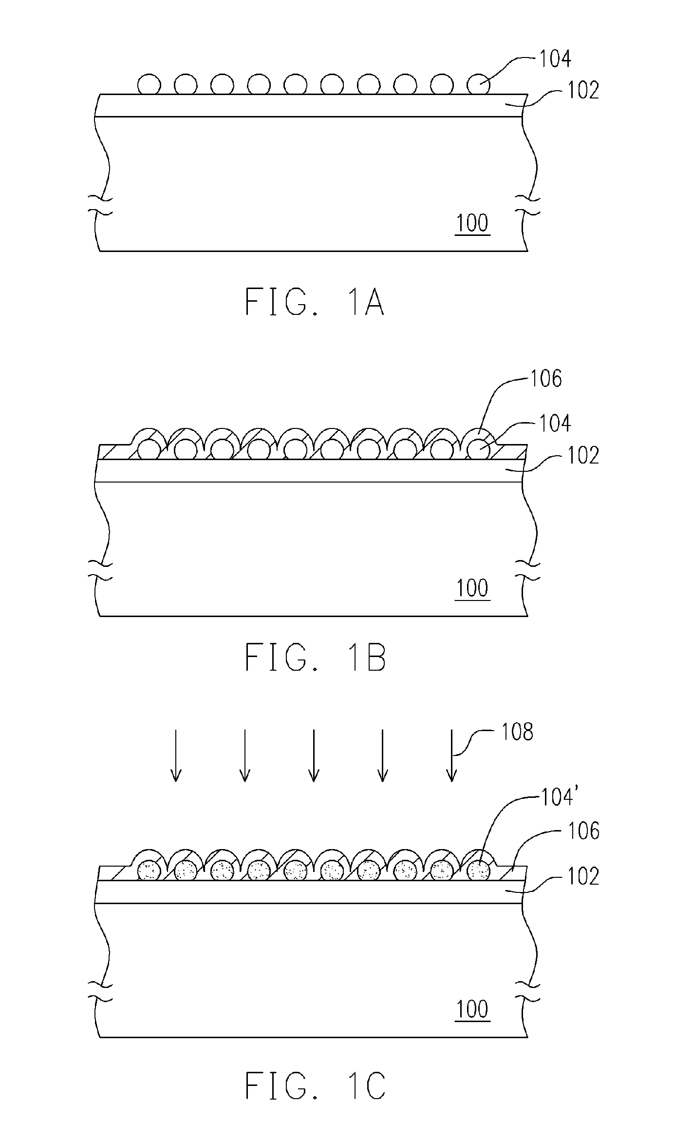
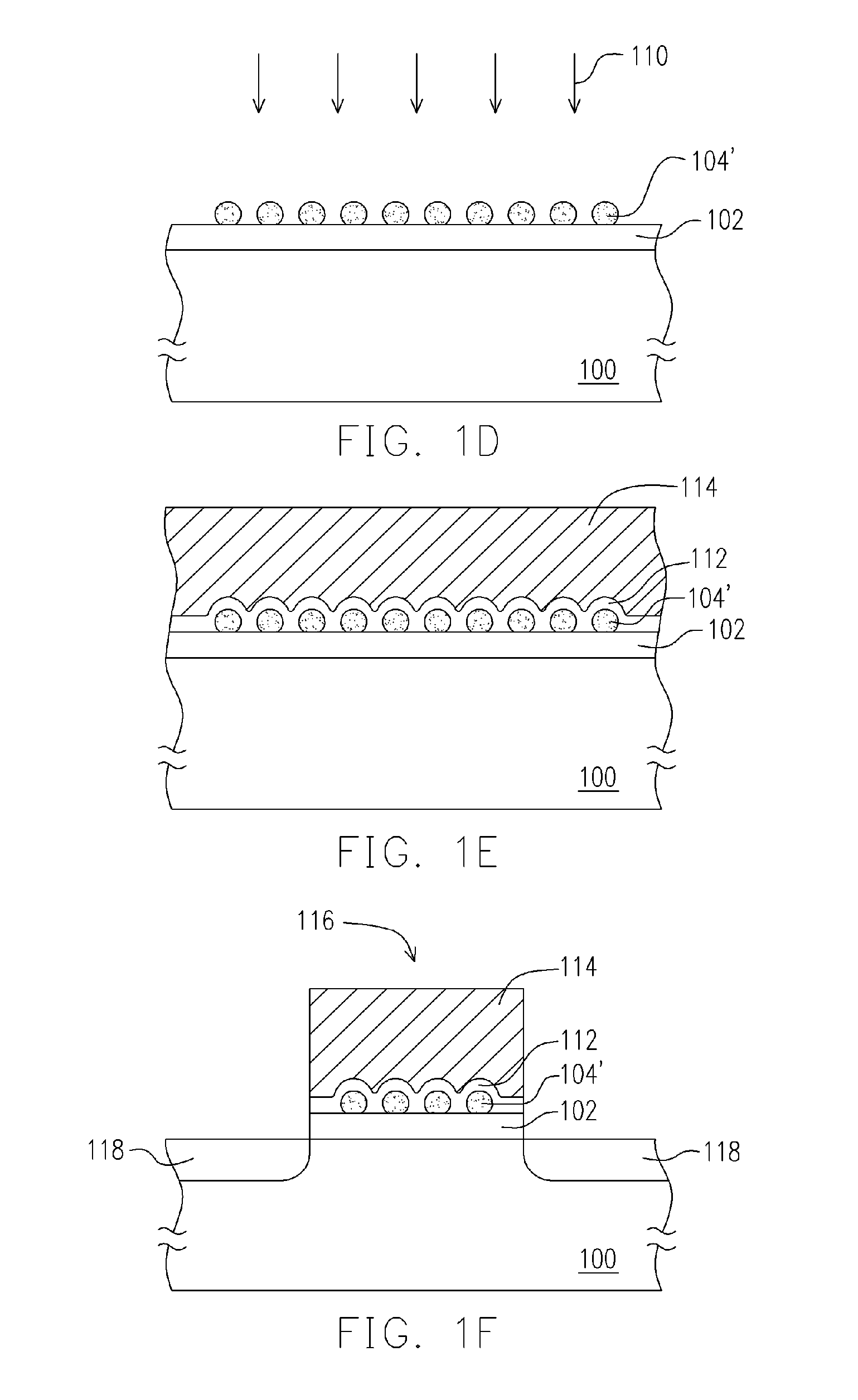
[0032]FIGS. 1A through 1F are schematic cross-sectional views showing the steps for producing a non-volatile memory according to one embodiment of the present invention. First, as shown in FIG. 1A, a substrate 100 is provided. The substrate 100 is a silicon substrate, for example. Then, a tunneling dielectric layer 102 is formed on the substrate 100. The tunneling dielectric layer 102 is a silicon oxide layer formed, for example, by performing a thermal oxidation process. Obviously, the tunneling dielectric layer 102 may also be fabricated by using some other suitable methods. Thereafter, a plurality of silicon nanocrystals 104 is formed on the tunneling dielectric layer 102. The silicon nanocrysta...


PUM

PropertyMeasurementUnit
dielectricaaaaaaaaaa
conductiveaaaaaaaaaa
metallicaaaaaaaaaa

Abstract

A method for manufacturing a non-volatile memory is provided. First, a tunneling dielectric layer is formed over a substrate. A plurality of silicon nanocrystals is formed on the tunneling dielectric layer. A silicide process is performed on the silicon nanocrystals to form a plurality of salicide nanocrystals. A dielectric layer and a conductive layer are sequentially formed on the substrate to cover the salicide nanocrystals and the tunneling dielectric layer. The conductive layer, the dielectric layer, the salicide nanocrystals and the tunneling dielectric layer are patterned to form a gate structure. A source/drain region is formed in the substrate on the respective sides of the gate structure.

Description

CROSS-REFERENCE TO RELATED APPLICATION [0001] This application claims the priority benefit of Taiwan application Ser. No. 94142751, filed on Dec. 05, 2005. All disclosure of the Taiwan application is incorporated herein by reference. BACKGROUND OF THE INVENTION [0002] 1. Field of the Invention [0003] The present invention relates to a method for manufacturing a memory. More particularly, the present invention relates to a method for manufacturing a non-volatile memory. [0004] 2. Description of the Related Art [0005] Memory is a semiconductor device specially designed for the storage of programs or data. Since non-volatile memory can retain stored data even after the power to the device is cut off, it has become an indispensable data storage element in many types of electronic products for holding normal start-up programs. In fact, it has become one of the most widely adopted memory devices in personal computer and electronic equipment. [0006] A typical non-volatile memory has floati...

Claims


Application Information

Patent Timeline
Patent Type & Authority Applications(United States)
IPC IPC(8): H01L21/336
CPCH01L27/105H01L27/11568H01L29/4925H10B43/30
Inventor CHU, CHIH-HSUN
Owner PROMOS TECH INC
Why Eureka
Try Eureka