Organic functional element and method for manufacturing same

a functional element and organic technology, applied in the field of organic functional elements, can solve the problems of limited method of vapor deposition of low-molecular materials with masks, consume almost the same power as in the full display state, and achieve the effects of easy expansion, low cost, and high reliability

Inactive Publication Date: 2007-06-14
DAI NIPPON PRINTING CO LTD
View PDF8 Cites 5 Cited by
  • Summary
  • Abstract
  • Description
  • Claims
  • Application Information

AI Technical Summary

Benefits of technology

[0065] According to the present invention, an electrode is formed on an organic material layer without using a vacuum film making method such as vapor deposition, whereby organic functional elements, particularly an organic EL element, an organic TFT element and the like can be manufactured. These functional elements can be large-sized easily and produced at lower cost. The organic material layer is not affected during formation of the electrode, and the organic functional element having high reliability without being affected by environmental changes can be realized.
[0066] The organic functional element of the present invention can be manufactured under vacuum or in an inert gas, and thus the emission uniformity of the light emitting surface can be further improved. The shape of the electrode can be arbitrarily regulated to further improving the degree of completion as the light emitting element. The element can also be completed by cooling and hardening a molten metal to close opening parts thereby simultaneously performing sealing.

Problems solved by technology

In the light receiving type display such as the LCD, the backlight is always lighted regardless of the mode of displayed information, thus consuming almost the same power as in the full displaying state.
This problem, on the other hand, hardly occurs in the self light emitting type display.
Among the methods described above, the method of vapor deposition of the low-molecular material with a mask is limited because of difficulty in large-sizing of the vacuum apparatus and the vapor deposition mask, so there is a problem of difficulty in large-sizing and in preparation of a large number of sheets by using large substrates.
This is not problematic for trial manufacture in the stage of development, but indicates poor competitiveness in the market in respect of tact and cost in the full-scale manufacturing stage.
In the manufacturing method described above, however, since the cathode is formed by vapor deposition, a large-scale vacuum apparatus is necessary only for this step, and for vacuum drawing, the production tact is delayed.
As a result, there is a problem that the characteristics of the organic EL material that can be coated to form a film cannot be fully utilized.
That is, when the melting point of the metal serving as an electrode is high, the high-temperature stability of the organic material layer at the time of forming the electrode is problematic, and a heating temperature significantly higher than the glass transition temperature of the organic material layer causes a problem of seriously affecting the organic material layer.
On the other hand, when the melting point of the metal serving as an electrode is low, the storage stability thereof as a functional element becomes problematic.
In an environment such as inside of automobile in summer, for example, the temperature inside the automobile is significantly increased, and when the organic EL element is used as a display apparatus where a low-melting metal serves as an electrode, there is a problem that the electrode is melted due to high temperatures to break the apparatus.
The alkali metal and alkaline earth metal in organic EL elements described in the patent documents 4, 5 and 6 are strongly oxidative, combustible and unstable in the air and are thus difficult to handle, so they can be formed into a film only under vacuum by vapor deposition, or the like.
This is because there is a problem that the electrode cannot be produced without using the vacuum vapor deposition process since the melting point of the metal used is high.

Method used


Image

  • Organic functional element and method for manufacturing same
  • Organic functional element and method for manufacturing same
  • Organic functional element and method for manufacturing same

Examples


example 1

[0141] The following solution was prepared in the example of the present invention.

[0142]

Polyvinyl carbazole70parts by weightOxadiazole compound30parts by weightFluorescent dye1part by weightMonochlorobenzene (solvent)4900parts by weight

[0143] When the fluorescent dye is coumarin 6, a green emission having a peak at 501 nm was obtained; in the case of perylene, a blue emission having a peak at 460 to 470 nm was obtained; and in the case of DCM (dicyanomethylene pyran derivative), a red emission having a peak at 570 nm was obtained. These were used as light emitting materials of the respective colors.

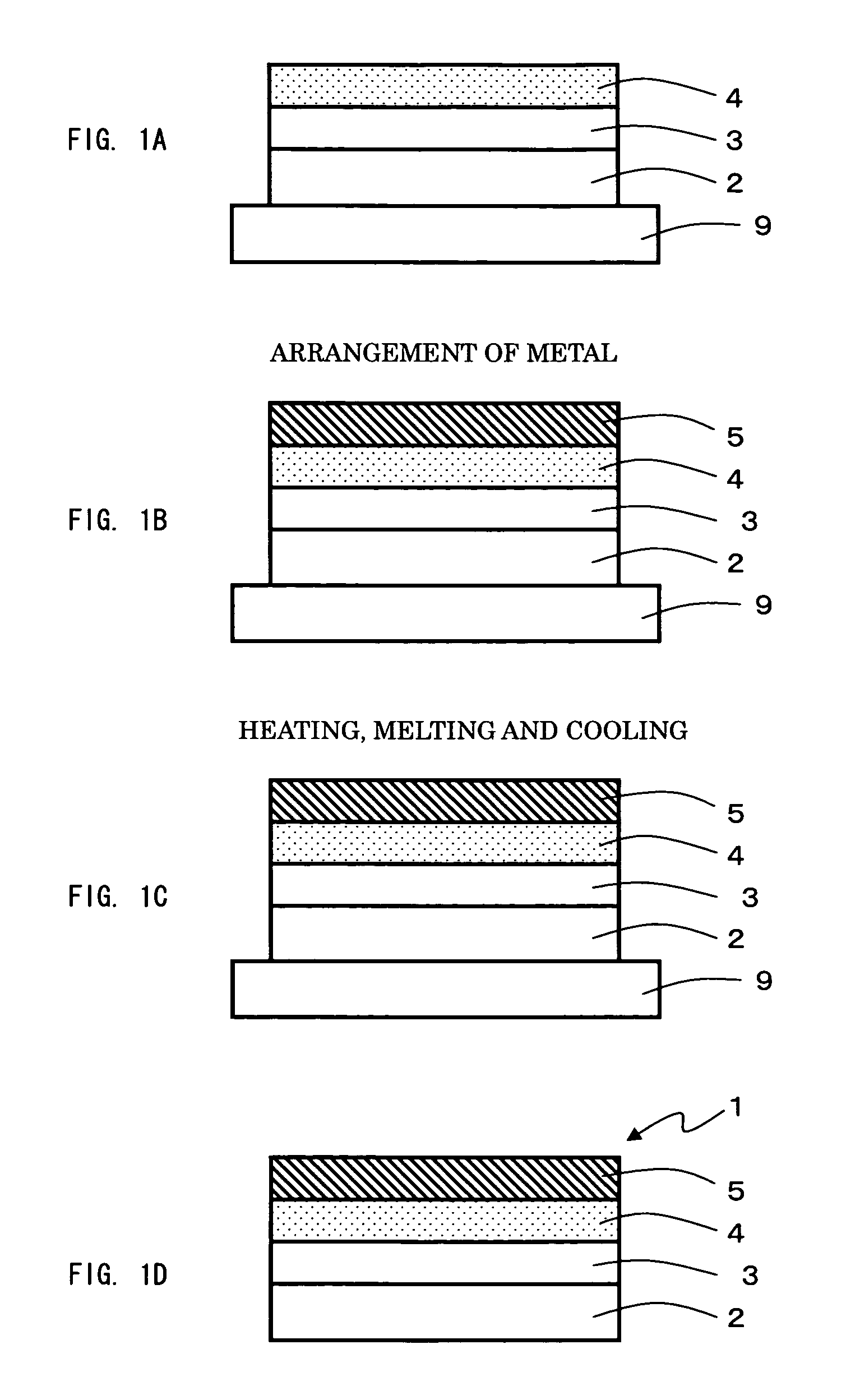
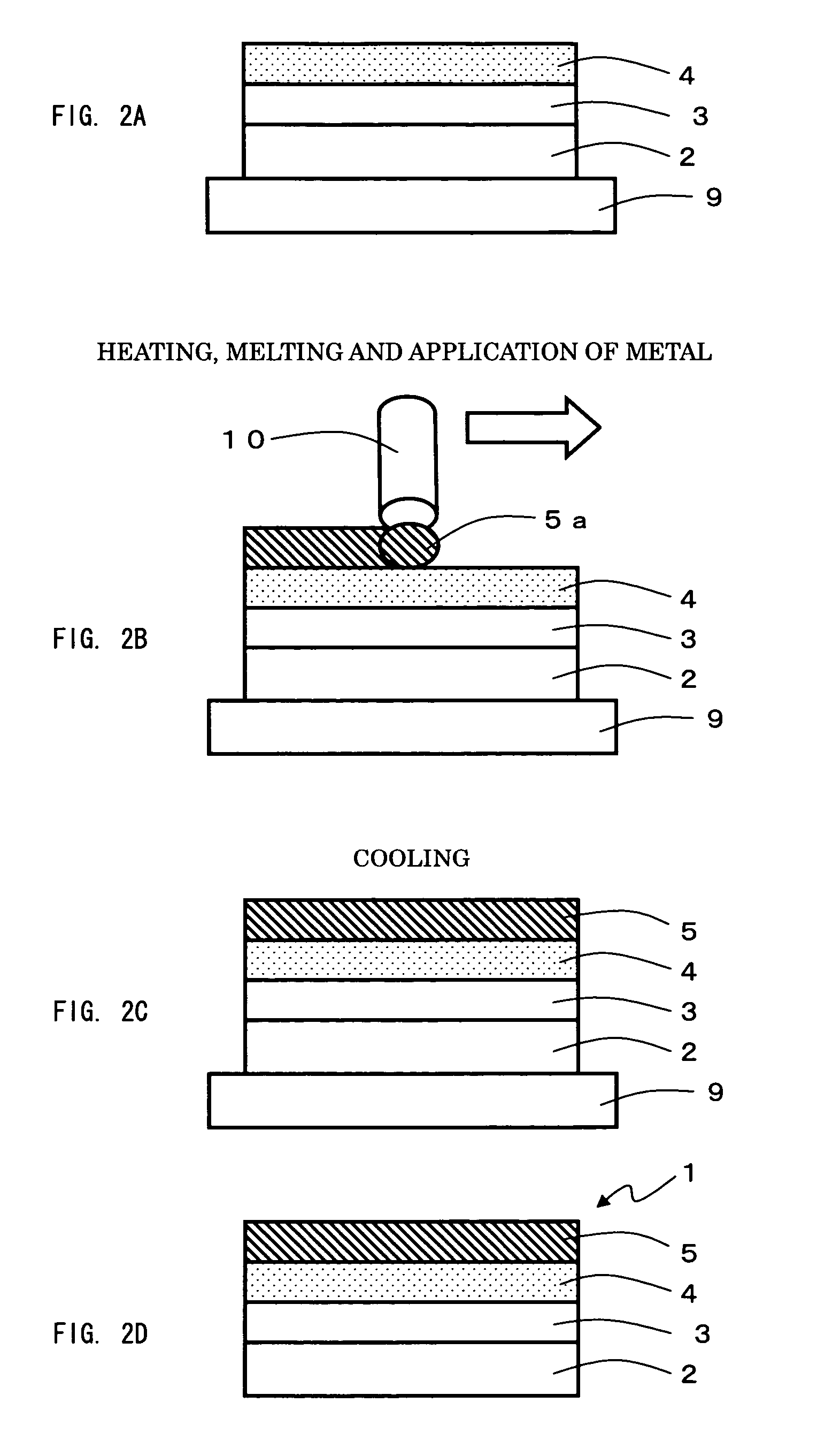
[0144] An organic EL element having a sectional shape shown in FIG. 9 was manufactured. A substrate 52 was glass, and a transparent electrode 53 was ITO of 200 nm in thickness. After the substrate 52 was washed, PEDOT / PSS (Bayer CH8000 manufactured by Bayer AG) was applied as a hole injection layer 56 to a thickness of 80 nm by spin coating and formed by baking at 160° C.

[0145] Then, ...

example 2

[0152] The same element as in Example 1 was manufactured except that the metal of the cathode was an alloy of Bi—Pb—Sn (50.0:31.2:18.8%).

example 3

[0153] The same element as in Example 1 was manufactured except that the metal of the cathode was an alloy of Bi—Pb—Sn (50.0:28.0:22.0%).


PUM

PropertyMeasurementUnit
glass transition temperatureaaaaaaaaaa
melting pointaaaaaaaaaa

Abstract

The object of the invention is to provide a highly reliable organic functional element such as an organic EL element or an organic semiconductor element exemplified by an organic TFT element which can be manufactured without requiring a vapor deposition process for forming an electrode on an organic material layer. Consequently, such an organic functional element can be large-sized easily and produced at lower cost. In addition, no damage is caused to the organic material layer during formation of the electrode, and the organic functional element is not affected by environmental changes. Also disclosed is a method for manufacturing such an organic functional element. To attain the above-mentioned object, the present invention provides an organic functional element comprising at least a plurality of electrodes and an organic material layer which is characterized in that at least one of the electrodes is composed of a metal having a melting point not higher than a temperature that is higher by 30° C. than the glass transition temperature of the organic material layer.

Description

TECHNICAL FIELD [0001] The present invention relates to an organic functional element, particularly an organic semiconductor element, an organic thin film transistor element (hereinafter, “thin film transistor” is referred to as “TFT”), an organic electroluminescence element (hereinafter, “electroluminescence” is referred to as “EL”), and a method for manufacturing the same. BACKGROUND ART [0002] In recent years, flat display apparatus (flat displays) are used in many fields and places, and have increasing importance with the progress of information technology. A typical example of the flat display at present is a liquid crystal display (also referred to as “LCD”), and as flat displays based on a displaying principle different from that of the LCD: an organic EL display, an inorganic EL display, a plasma display panel (also referred to as “PDP”), a light emitting diode display apparatus (also referred to as “LED”), a vacuum fluorescent display apparatus (also referred to as “VFD”), ...

Claims


Application Information

Patent Timeline
Patent Type & Authority Applications(United States)
IPC IPC(8): H01B1/12H01L51/00H05B33/26H01L51/05H01L51/40H01L51/50H01L51/52H05B33/04H05B33/10
CPCH01L51/0003H01L51/0021H01L51/0512H01L51/5203H10K71/12H10K71/60H10K10/462H10K50/82
Inventor ITO, NOBOYUKI
Owner DAI NIPPON PRINTING CO LTD
Why Eureka
Try Eureka