Unipolar resistance random access memory (RRAM) device and vertically stacked architecture

a random access memory and unipolar resistance technology, applied in the direction of digital storage, galvano-magnetic devices, instruments, etc., can solve the problems of limited application of vertically stacked memories, pcram is not compatible with this architecture, and poly-silicon diodes require about 750 c during fabrication, so as to achieve high performance

Inactive Publication Date: 2007-06-14
HITACHI GLOBAL STORAGE TECH NETHERLANDS BV
View PDF19 Cites 542 Cited by
  • Summary
  • Abstract
  • Description
  • Claims
  • Application Information

AI Technical Summary

Benefits of technology

[0020] The present invention provides a low-cost, high-performance, rewritab

Problems solved by technology

However, these vertically stacked memories have limited application because they cannot be rewritten.
However, PCRAM is not compatible with this architecture for two main reasons.
First, poly-silicon diodes require about 750 C during fabrication, a temperature at which typical phase change materials are unstable.
When a larger (write) voltage is applied, charge may be trapped in a high energy configuration due to the presence of defects such as dangling bonds.
Flash memory, based on storing charge on the floating gate of a transistor, has very serious scaling challenges because the dielectric around the floating gate must be at least 8 nanometers (nm) thick to retain charge for ten years.
This can make it difficult for the floating

Method used


Image

  • Unipolar resistance random access memory (RRAM) device and vertically stacked architecture
  • Unipolar resistance random access memory (RRAM) device and vertically stacked architecture
  • Unipolar resistance random access memory (RRAM) device and vertically stacked architecture

Examples


Embodiment Construction

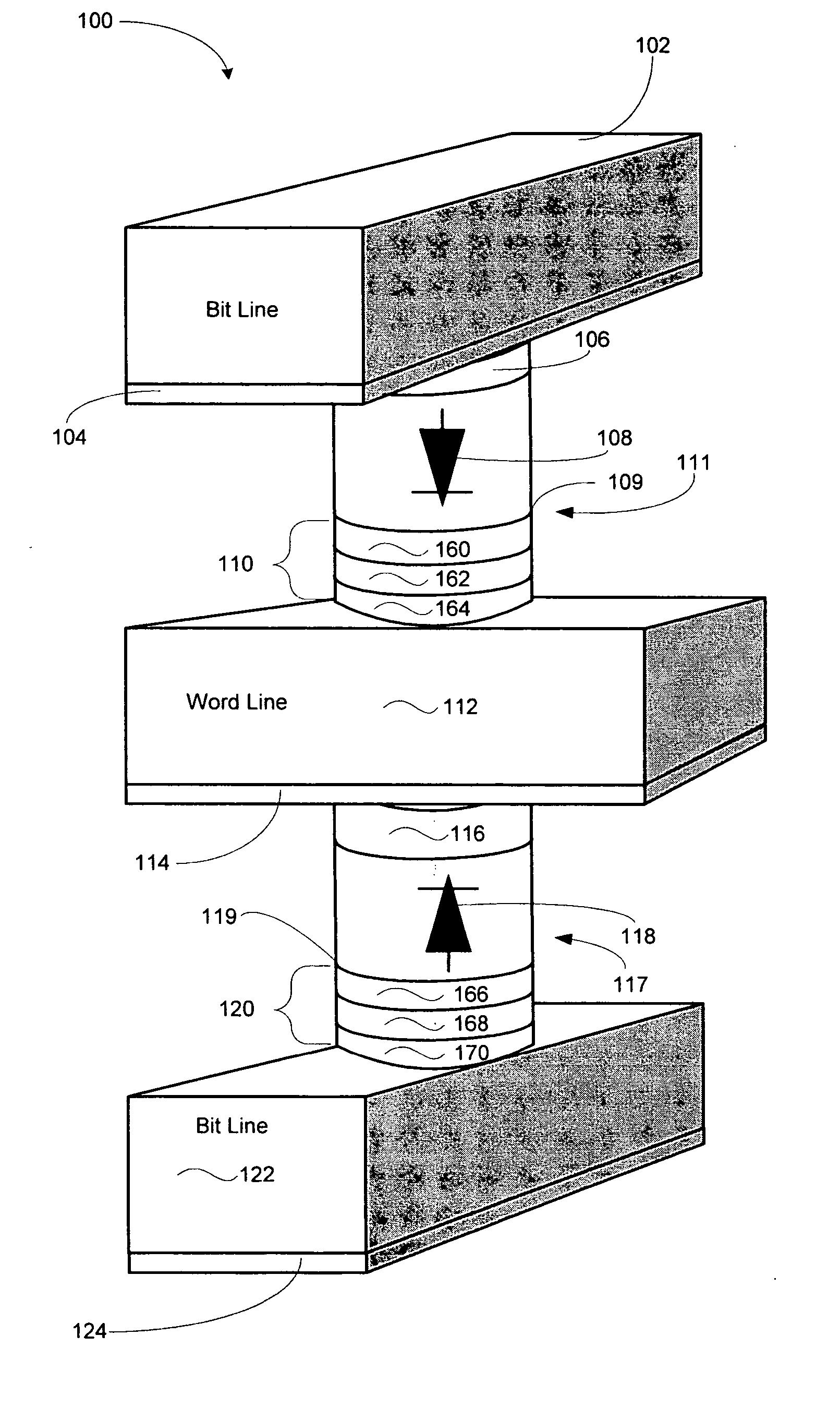
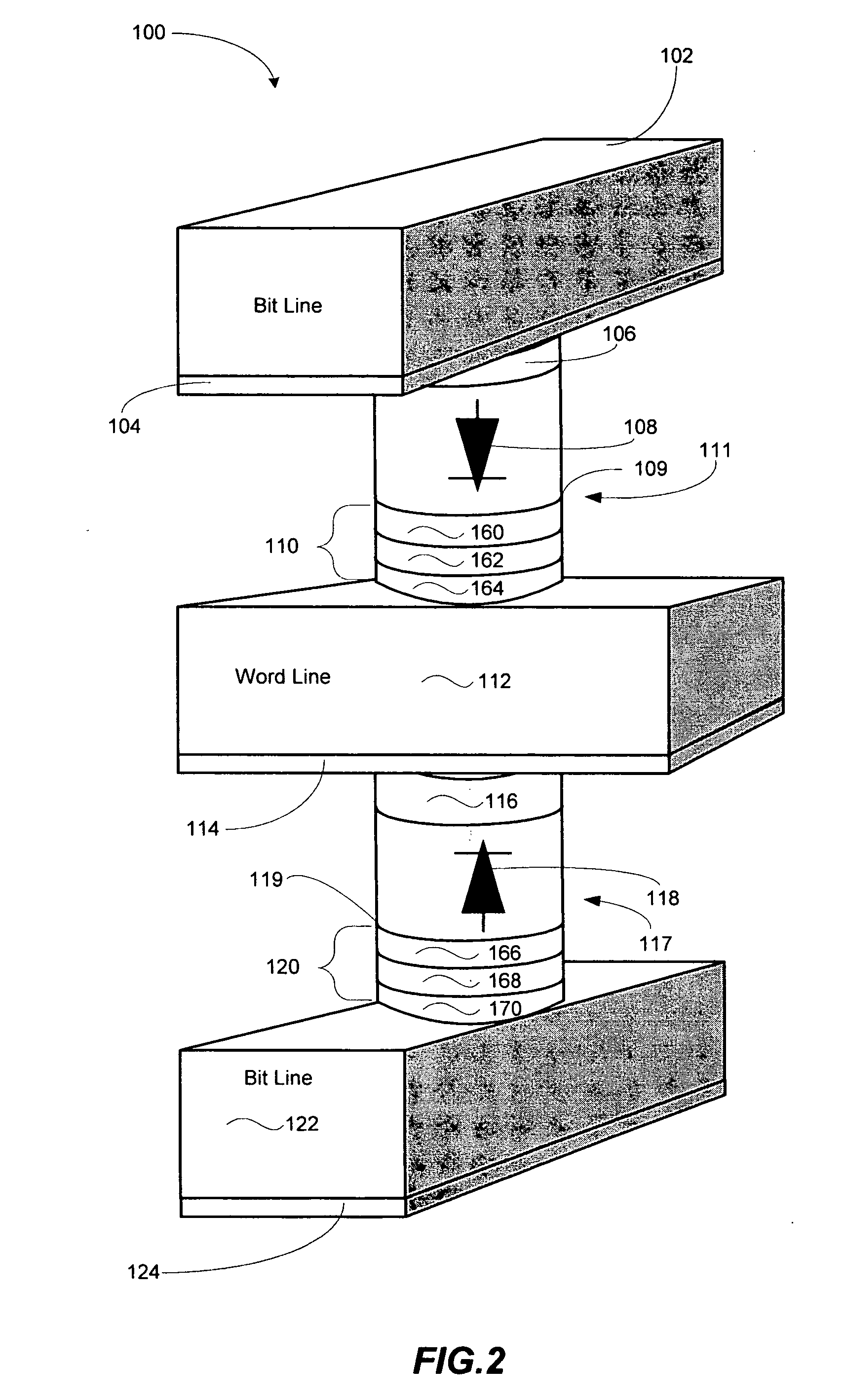
[0033] As known in the art, large cross-point arrays of memory cells may be formed and stacked vertically on top of one another. For example, the arrays may be formed by 8192 word lines in layer 1, 128 perpendicular bit lines in layer 2, 8192 word lines in layer 3, 128 bit lines in layer 4, and on up to 8192 word lines in layer 9. Memory cells are formed at the intersections of bit lines and word lines to form 8 layers of memory cells. Thus, the 3-dimentional array includes eight million memory cells and a large number of arrays may be included on a semiconductor die.

[0034] Within each memory cell is a RRAM device, as previously described, and a poly-silicon diode. Diodes point in opposite directions in vertically adjacent memory layers so that current may flow from each bit line to any of the 16384 word lines directly above or below the bit line. Accordingly, bit lines and word lines are “shared” (expect for the bottom-most word line and top-most word line which are typically conn...


PUM


Abstract

One embodiment of the present invention includes a low-cost unipolar rewritable variable-resistance memory device, made of cross-point arrays of memory cells, vertically stacked on top of one another and compatible with a polycrystalline silicon diode.

Description

BACKGROUND OF THE INVENTION [0001] 1. Field of the Invention [0002] This invention relates generally to the field of solid state (or non-volatile) ultra-low-cost mass storage device (or memories) based on a low current, vertically-stacked unipolar resistance random access memory (RRAM) and in particular, to a three-dimensional (3-D) cross point arrangement of memory cells forming a ultra-low-cost solid state memory or mass storage device made of low-current vertically-stacked unipolar RRAM. [0003] 2. Description of the Prior Art [0004] Today, three-dimensional programmable read-only memories (PROMs) based on polycrystalline silicon (poly-Si) diodes and write-once antifuses, are gaining notoriety in commercial applications having the advantage of being less expensive than the current low-cost leader in rewritable solid state memory, i.e. two bit-per-cell NAND flash. For further details regarding this subject matter, the reader is referred to “512 Mb PROM With 8 Layers of Antifuse / Dio...

Claims


Application Information

Patent Timeline
IPC IPC(8): H01L43/00
CPCG11C13/0007G11C2213/31G11C2213/34G11C2213/71G11C2213/72H01L27/101H01L27/2409H01L27/2481H01L45/1233H01L45/145H01L45/146H01L45/04H10B63/20H10B63/84H10N70/20H10N70/826H10N70/8833H10N70/883
Inventor STIPE, BARRY CUSHING
Owner HITACHI GLOBAL STORAGE TECH NETHERLANDS BV
Why Eureka
Try Eureka